
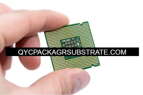
SHDBU Substrate Manufacturer. the Package Substrate will be made with Showa Denko and Ajinomoto High speed materials.or other types high speed materials and high frequency materials.
SHDBU substrates, an acronym for “super high density buried undercut” substrates, represent an innovative semiconductor substrate technology utilized in the manufacturing of cutting-edge integrated circuits (ICs). These substrates are engineered to minimize parasitic capacitance, thereby bolstering IC performance, notably in high-frequency applications such as RF and microwave circuits.
At the heart of SHDBU substrates lies a buried undercut region positioned beneath the active device areas. This distinctive structural feature enables a more compact arrangement of components and interconnections while curtailing parasitic capacitance between neighboring elements. Consequently, SHDBU substrates contribute to heightened signal integrity and amplified operational frequencies in ICs.
The fabrication process of SHDBU substrates entails employing specialized semiconductor manufacturing techniques, including epitaxial growth and selective etching. These sophisticated processes are pivotal in creating the buried undercut region beneath the active device areas, facilitating the integration of components at increased densities on the substrate.
In essence, SHDBU substrates serve as a cornerstone in advancing the performance metrics of ICs, particularly in scenarios where signal integrity and operational frequency are of paramount importance.
What can SHDBU Substrates do?
SHDBU substrates bring a host of capabilities to the table, elevating the performance of integrated circuits:
Capacitance Reduction: With a buried undercut region strategically positioned beneath active device areas, SHDBU substrates effectively diminish parasitic capacitance between components. This reduction not only bolsters signal integrity but also slashes signal propagation delays, particularly advantageous for applications demanding high-frequency precision.
Density Enhancement: Thanks to their ingenious design, SHDBU substrates facilitate a denser arrangement of devices and interconnections. This translates into the integration of a greater number of components within a smaller footprint, paving the way for heightened functionality on a single chip.
Frequency Amplification: By curbing parasitic capacitance and enabling compact integration, SHDBU substrates empower the creation of integrated circuits capable of operating at elevated frequencies. This makes them indispensable for applications such as RF and microwave circuits, where top-tier frequency performance is paramount.
Efficiency Boost: The streamlined layout and minimized parasitic capacitance of SHDBU substrates lead to improved power efficiency in integrated circuits. This is a game-changer in sectors prioritizing energy conservation, such as mobile technology and wireless communication systems.
In essence, SHDBU substrates serve as a cornerstone for enhancing integrated circuit capabilities, offering advantages like superior signal integrity, increased frequency range, enhanced integration densities, and optimized power efficiency.
What are the advantages of SHDBU Substrates?
SHDBU substrates, standing for Super High Density Board Units, bring about several benefits within the realm of electronic packaging and the semiconductor industry. Let’s delve into these advantages:
Elevated Wiring Density: SHDBU substrates outshine traditional counterparts by boasting a significantly heightened wiring density. This characteristic facilitates the creation of more condensed electronic device designs, making them ideal for contemporary, downsized electronic configurations.
Enhanced Signal Integrity: The densely packed wiring in SHDBU substrates works wonders in mitigating signal interference and crosstalk between adjacent traces. This results in a marked improvement in signal integrity, a pivotal aspect, especially in applications demanding high-speed and high-frequency performance.
Optimized Thermal Performance: SHDBU substrates often incorporate sophisticated thermal management features, including embedded heat sinks, vias, or metal layers. These elements efficiently dissipate heat, addressing thermal challenges in high-powered electronic devices and elevating overall reliability and performance.
Streamlined Component Integration: The compact nature of SHDBU substrates allows for seamless integration of various components, such as microprocessors and memory chips, onto a single substrate. This streamlines the assembly process and reduces the overall footprint of the final electronic system.
Cost-Effective Solutions: Despite their advanced technology, SHDBU substrates can offer cost efficiencies in specific applications. This is attributed to their capability to consolidate components, streamline assembly procedures, and enhance overall system performance, thus balancing out initial material costs.
Tailored Customization and Design Flexibility: SHDBU substrates lend themselves to customization based on specific design requirements. This includes considerations for layer counts, materials, and manufacturing processes. This flexibility empowers designers to optimize the substrate for their unique applications, leading to superior overall system performance.
Seamless Compatibility with Advanced Packaging Technologies: SHDBU substrates seamlessly align with various advanced packaging technologies, such as flip-chip, chip-on-board, and system-in-package. This alignment empowers designers to harness these technologies, enhancing overall system performance and functionality.
In essence, SHDBU substrates present a compelling solution for electronic packaging applications where high-density interconnects, improved thermal performance, and design flexibility take center stage.
What is the relationship between SHDBU Substrates and IC packaging?
SHDBU substrates and IC (Integrated Circuit) packaging are intricately linked elements in the intricate landscape of electronic devices, particularly within the expansive domain of the semiconductor industry. The nuanced dance between SHDBU substrates and IC packaging revolves around their collective roles in orchestrating the functionality and performance of integrated circuits. Here, we unravel the nuanced dimensions of their interconnected dynamics:
Pivotal Mounting and Interconnectivity: SHDBU substrates stand as the bedrock for mounting and interconnecting an array of electronic components, ICs included. They serve as a robust stage for seamlessly integrating these components, choreographing the intricate dance of wiring and connectivity.
Wiring Density and Signal Prowess: The superlative wiring density of SHDBU substrates assumes a central role in safeguarding signal integrity within electronic devices. This becomes particularly critical in the realm of high-speed ICs, where the efficient transmission of signals is paramount. The densely interwoven connections on SHDBU substrates act as custodians, minimizing signal interference and crosstalk.
Adept Thermal Governance for ICs: The operational heat generated by ICs demands deft thermal management for optimal functionality and reliability. SHDBU substrates artfully incorporate advanced thermal management features, such as embedded heat sinks and vias, facilitating the graceful dissipation of heat and preserving conducive operating temperatures for ICs.
Harmonious Contribution to Miniaturization and Component Fusion: SHDBU substrates take center stage in the ongoing narrative of electronic device miniaturization. They play a crucial role in seamlessly integrating an array of components, ICs being integral to this ensemble, onto a singular substrate. This synchronizes with the industry’s thrust towards diminished form factors and heightened component fusion, amplifying the overall efficiency of IC packaging.
Synchronization with Advanced IC Packaging Technologies: SHDBU substrates are meticulously crafted to synchronize effortlessly with a diverse array of advanced IC packaging technologies. This includes the intricacies of flip-chip, chip-on-board, and system-in-package methodologies. This seamless synchronization augments the overall flexibility and efficiency of the IC packaging process.
Customization Crafted for IC Exigencies: SHDBU substrates unveil a canvas of customization, meticulously tailored to meet the unique exigencies of IC designs. This bespoke approach encompasses considerations ranging from layer count to material intricacies and overall layout finesse. The result is a bespoke tapestry, finely tuned to optimize the performance and reliability of ICs.
In summation, SHDBU substrates and IC packaging share an intertwined existence in the narrative of electronic device evolution. SHDBU substrates take on the mantle of providing a robust canvas for mounting and interconnecting ICs, offering a symphony of heightened wiring density, signal integrity, thermal mastery, and customization, attuned to the dynamic cadence of evolving IC designs.
How do SHDBU Substrates differ from traditional PCBs?
SHDBU substrates carve out a distinctive niche when compared to conventional PCBs (Printed Circuit Boards), showcasing a range of features that set them apart. Let’s unravel the divergences that distinguish SHDBU substrates from their more traditional counterparts:
Wiring Density Prowess: The standout feature lies in the remarkable wiring density of SHDBU substrates, far surpassing that of traditional PCBs. This intricate web of connections allows for a more compact design, aligning seamlessly with the demands of contemporary electronic devices.
Signal Integrity Emphasis: SHDBU substrates prioritize signal integrity with their elevated wiring density. This not only minimizes signal interference but also curtails crosstalk between traces, ensuring a robust and dependable signal transmission. Traditional PCBs, with lower wiring density, may struggle to attain comparable levels of signal integrity.
Advanced Thermal Management Integration: SHDBU substrates often integrate advanced thermal management features, such as embedded heat sinks and vias. This sophisticated thermal architecture facilitates more efficient heat dissipation, catering to the thermal challenges inherent in high-powered electronic devices. In contrast, traditional PCBs may lack these advanced thermal solutions.
Miniaturization Expertise and Component Fusion: A pivotal role played by SHDBU substrates is their support for the ongoing trend of electronic device miniaturization. They facilitate heightened integration of components onto a singular substrate, contributing to the pursuit of smaller form factors. Traditional PCBs may grapple with achieving comparable levels of miniaturization and component integration.
Harmonious Compatibility with Advanced Packaging Technologies: SHDBU substrates are intricately designed to seamlessly mesh with a variety of advanced packaging technologies, including flip-chip and system-in-package methodologies. This adaptability enhances their versatility in meeting the evolving needs of electronic packaging. Traditional PCBs, by nature, may lack the same level of adaptability to cutting-edge packaging methods.
Flexibility in Customization: SHDBU substrates offer an elevated degree of customization. Designers can tailor the substrate to specific requirements, encompassing considerations such as diverse layer counts, varied materials, and distinct manufacturing processes. This flexibility provides designers with a broader spectrum of options to fine-tune the substrate for specific applications, a facet that is often more constrained in traditional PCBs.
Cost Dynamics: While the upfront costs of SHDBU substrates may be higher due to their advanced technology, they can present cost efficiencies over time. The ability to consolidate components, streamline assembly processes, and enhance overall system performance may offset initial material costs in the long run.
In essence, SHDBU substrates emerge as pioneers in electronic packaging technology, offering a suite of advantages in wiring density, signal integrity, thermal management, miniaturization, and customization when juxtaposed with traditional PCBs.
What are the manufacturing technologies of SHDBU Substrates?
Crafting SHDBU substrates involves a sophisticated fusion of advanced manufacturing technologies, each contributing to the distinct characteristics that set these substrates apart. Here’s an exploration of the key manufacturing technologies that contribute to the creation of SHDBU substrates:
Precision Lithography for Delicate Patterns: SHDBU substrates demand meticulous attention to detail in the patterning of fine lines and spaces. To achieve this, advanced lithography techniques, including photolithography and electron beam lithography, are employed with precision to etch intricate circuitry onto the substrate surface with sub-micron accuracy.
Strategic Multilayer Assembly: SHDBU substrates leverage multilayer build-up technology to accommodate an abundance of interconnections within a confined space. This involves the strategic stacking of multiple layers of conductive and insulating materials, allowing for the creation of complex interconnect structures.
Embedded Component Integration Expertise: SHDBU substrates often incorporate embedded components directly into the substrate material. This involves the seamless integration of passive elements like resistors and capacitors or, in some cases, active components such as semiconductor chips. This integration occurs harmoniously during the manufacturing process.
Utilization of Cutting-edge Dielectric Materials: Superior dielectric materials, engineered for exceptional thermal and electrical properties, play a pivotal role in SHDBU substrates. These materials may include specialized ceramics, polymers, or composite materials designed to meet stringent performance criteria.
Innovative Microvia and Via-in-Pad Approaches: Achieving high-density interconnects without compromising signal integrity is a key challenge addressed through innovative microvia and via-in-pad technology. These methods involve precision drilling of small-diameter vias or the placement of vias directly within component pads, facilitating efficient signal routing through the substrate layers.
Incorporation of Thermal Management Ingenuity: Various thermal management solutions are seamlessly woven into SHDBU substrates to efficiently dissipate the heat generated by electronic components. This can include the integration of embedded heat sinks, thermal vias, metal-core layers, or specialized dielectric materials with enhanced thermal conductivity.
Tailored Customization for Precision Design: SHDBU substrates offer an exceptional level of customization to align with the nuances of specific design requirements. Leveraging advanced manufacturing technologies, designers can tailor substrate materials, layer configurations, surface finishes, and other parameters, ensuring optimal performance for diverse application needs.
In essence, the manufacturing of SHDBU substrates is a nuanced orchestration of precision lithography, intricate material assembly, embedded component integration, and thermal management finesse. This amalgamation results in the creation of high-performance electronic packaging solutions meticulously crafted to cater to the demands of varied applications.
Frequently Asked Questions (FAQs)
What does SHDBU stand for?
SHDBU stands for “super high density buried undercut.”
What are SHDBU substrates used for?
SHDBU substrates find application in the production of high-performance integrated circuits (ICs), particularly in scenarios where signal integrity and high-frequency operation are paramount, such as RF and microwave circuits.
What advantages do SHDBU substrates offer?
SHDBU substrates provide several benefits, including reduced parasitic capacitance, increased integration densities, enhanced signal integrity, improved operational frequencies, and better power efficiency within ICs.
What materials are typically used in SHDBU substrates?
SHDBU substrates are commonly made of semiconductor materials like silicon or gallium arsenide (GaAs).
How do SHDBU substrates differ from traditional PCBs?
Unlike traditional PCBs, which serve general electronic interconnection and support purposes, SHDBU substrates are specifically designed for high-performance ICs, featuring specialized structures like buried undercut regions to minimize parasitic capacitance.
What role do SHDBU substrates play in IC packaging?
While SHDBU substrates serve as the basis for IC integration, IC packaging encases ICs in protective housings, enabling electrical connections, heat dissipation, and signal integrity enhancement.
Conclusion
In closing, SHDBU substrates mark a significant leap forward in semiconductor innovation. Engineered for top-tier integrated circuits (ICs), these substrates deliver a host of advantages, including reduced parasitic capacitance, heightened integration densities, enhanced signal fidelity, increased operational frequencies, and superior energy efficiency.
Crafted through a meticulous process involving specialized semiconductor fabrication techniques like epitaxial growth, selective etching, planarization, doping and ion implantation, metallization, and photolithography, SHDBU substrates form the cornerstone of advanced IC development. They excel particularly in applications requiring precise signal integrity and high-frequency performance.
Primarily fashioned from semiconductor materials like silicon or gallium arsenide (GaAs), SHDBU substrates stand apart from traditional printed circuit boards (PCBs) by their tailored design for high-speed, high-frequency IC applications. Notably, they feature specialized structural elements such as buried undercut regions.
While SHDBU substrates lay the groundwork for IC integration, IC packaging plays a complementary role by providing protective housing, electrical connectivity, thermal management, and signal enhancement.
In essence, SHDBU substrates represent a pivotal stride forward in semiconductor technology, empowering the realization of advanced ICs with unmatched performance and functionality.