
What is Ultra-Small Spacing Substrates?
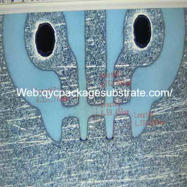
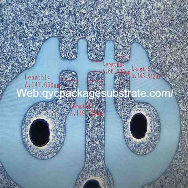
Ultra-Small Spacing Substrates manufacturer. we can produce the best samllest bump pitch with 100um, the best smallest microtrace are 9um. and the smallest gap are 9um. we can use the rogers base. BT base. and other base materials to do the microtrace/spacing HDI PCBs with high quality and fast lead time.
As of my last knowledge update in January 2022, there might not be a widely recognized term specifically referring to “Ultra-Small Spacing Substrates.” However, it’s possible that new technologies and terminologies have emerged since then. I’ll provide information based on the general understanding of high-density, compact boards with a tiny pitch, which could be relevant to your question.
High-Density and Compact Design:
Ultra-small spacing substrates typically refer to circuit boards or substrates that have extremely tight spacing between components and traces.
These substrates are characterized by a high component density and a compact design, allowing for more electronic components to be placed within a smaller area.
Tiny Pitch:
The “pitch” refers to the distance between two corresponding features on a substrate, such as the distance between two solder balls or the spacing between traces.
Ultra-small spacing substrates have a tiny pitch, meaning that the distance between various elements on the board, such as solder pads or traces, is significantly reduced compared to traditional circuit boards.
Advantages for Advanced Electronic Devices:
Miniaturization: The primary advantage of ultra-small spacing substrates is the ability to create smaller and lighter electronic devices. This is crucial for applications where size and weight constraints are significant factors, such as portable electronics and wearable devices.
Improved Performance: The reduced distances between components can lead to shorter signal paths, minimizing signal delays and improving overall performance.
High-Speed Applications: These substrates are often suitable for high-speed electronic applications, such as advanced processors and communication devices, where signal integrity is critical.
Chip Packaging Technologies:
3D Integration: Ultra-small spacing substrates are often associated with advanced chip packaging technologies, including 3D integration. This involves stacking multiple semiconductor dies vertically to enhance performance and reduce the overall footprint of the device.
Advanced Packaging Techniques: These substrates are commonly used in advanced packaging techniques like fan-out wafer-level packaging (FOWLP) and system-in-package (SiP) to achieve higher integration levels and improved thermal performance.
Challenges:
Manufacturing Precision: The manufacturing of ultra-small spacing substrates requires high precision in both design and manufacturing processes to ensure the reliability of the final product.
Thermal Management: As components are packed more densely, thermal management becomes a critical concern. Efficient heat dissipation solutions are essential to prevent overheating.
In summary, ultra-small spacing substrates are designed to meet the demands of miniaturization and high-performance requirements in advanced electronic devices. Ultra-small spacing substrates play a vital role in facilitating the creation of compact and high-performance electronic devices, especially in scenarios where spatial limitations are a key concern. It’s important to note that terminology and technologies may have advanced since my last update in January 2022, so staying informed with the latest developments is advisable.
How Do Ultra-Small Spacing Substrates Function?
Ultra-small spacing substrates primarily function as essential components in miniature electronic devices, providing crucial support and connectivity. The key aspects of their functioning include high-density wiring and a minute pitch, both of which contribute to enhancing overall performance. Here’s a detailed exploration:
Support for Miniature Electronic Devices:
Compact Design: Ultra-small spacing substrates are designed to accommodate a high concentration of electronic components within a limited space, enabling the creation of compact and miniature devices.
Structural Integrity: Despite their small size, these substrates must maintain structural integrity to support the mounting of various components such as integrated circuits, resistors, and capacitors.
Connectivity Enhancement:
Reduced Signal Path Lengths: The tiny pitch and high-density wiring on these substrates contribute to shorter signal paths between components. This reduction in distance minimizes signal propagation delays, enhancing the overall speed and efficiency of electronic devices.
Improved Signal Integrity: The close proximity of traces and components helps mitigate signal interference and crosstalk, resulting in improved signal integrity and reliability.
High-Density Wiring:
Increased Component Density: The high-density wiring allows for a greater number of components to be integrated into the substrate, supporting the development of complex electronic circuits in a confined space.
Enhanced Functionality: With more components densely packed, electronic devices can offer advanced functionalities, making them suitable for applications that demand sophisticated features in a small form factor.
Minute Pitch:
Space Efficiency: The minute pitch, referring to the reduced distance between features like solder pads or traces, contributes to the efficient use of space on the substrate. This is crucial for meeting the size constraints of modern electronic devices.
Facilitates Advanced Packaging Techniques: The tiny pitch is often associated with advanced packaging techniques, such as fine-pitch ball grid array (BGA) configurations, allowing for increased interconnect density and improved thermal performance.
Performance Enhancement:
Shorter Interconnections: The minimized distances between components result in shorter interconnections, reducing electrical resistance and capacitance. This, in turn, supports higher data transfer rates and lower power consumption.
Thermal Management: The compact design, along with the minute pitch, aids in efficient thermal management by enabling heat to dissipate more effectively, ensuring optimal operating conditions for electronic components.
In summary, the primary function of ultra-small spacing substrates lies in supporting and connecting miniature electronic devices. Their high-density wiring and minute pitch play integral roles in enhancing overall device performance by reducing signal path lengths, improving signal integrity, increasing component density, and promoting efficient use of space. These features collectively contribute to the development of smaller, yet more powerful, electronic devices.
What Types of Ultra-Small Spacing Substrates Exist?
Ultra-small pitch substrates, within the category of package substrates, exhibit distinct features that set them apart and contribute to their versatility across various applications. Their unique characteristics make them a driving force in printed circuit board (PCB) innovation, catering to diverse sectors ranging from consumer electronics to industrial applications. Here’s an exploration of the versatility of ultra-small pitch substrates:
Consumer Electronics: Ultra-small pitch substrates play a crucial role in the miniaturization of consumer electronics. In smartphones, tablets, wearables, and other portable devices, these substrates enable the compact arrangement of components, contributing to sleek designs and enhanced functionality.
In the field of high-performance computing, where emphasis is placed on power efficiency and optimal performance, ultra-small pitch substrates play a pivotal role. They enable the seamless integration of densely packed components, a critical factor for applications in data centers, supercomputers, and high-speed computing systems.
Automotive Electronics: The automotive industry benefits from the versatility of ultra-small pitch substrates in electronic control units (ECUs), sensors, and infotainment systems. Their compact design supports the space constraints within vehicles while contributing to the reliability and performance of automotive electronics.
Medical Devices: In the field of medical devices, where precision and reliability are critical, ultra-small pitch substrates find application in devices such as implantable medical devices, diagnostic equipment, and portable medical devices. Their miniaturization capabilities contribute to the development of advanced and compact medical technologies.
Industrial Applications: Ultra-small pitch substrates are employed in industrial settings for various applications, including control systems, monitoring devices, and automation equipment. Their capacity to endure challenging environmental conditions, coupled with their capability to provide high-density interconnections, renders them well-suited for deployment in industrial electronics.
IoT (Internet of Things): The expanding realm of the Internet of Things (IoT) relies significantly on ultra-small pitch substrates to facilitate the creation of compact, interconnected devices. These substrates play a crucial role in enabling the design of IoT sensors and devices with minimized form factors, thereby driving the proliferation of IoT applications across diverse industries.
Aerospace and Defense: In aerospace and defense applications, where both size and reliability are critical, ultra-small pitch substrates are utilized in avionics, radar systems, and communication equipment. Their compact design contributes to weight reduction and efficient use of space in aerospace electronics.
Wearable Technology: Ultra-small pitch substrates play a crucial role in enhancing wearables, such as smartwatches and fitness trackers. Their capability to support the miniaturization of components allows for the creation of lightweight and compact wearables without compromising performance. These substrates contribute significantly to the design and functionality of wearable devices, ensuring a balance between size reduction and optimal performance.
Telecommunications: In the telecommunications industry, ultra-small pitch substrates are employed in the development of high-speed communication equipment, routers, and networking devices. Their high-density interconnects contribute to the efficient transmission of data in telecommunications infrastructure.
In summary, the adaptability of ultra-small pitch substrates lies in their capacity to facilitate miniaturization, support high-density interconnects, and integrate advanced manufacturing techniques. Their versatility has far-reaching implications across various industries, propelling advancements in electronic device design and playing a pivotal role in the creation of more compact, efficient, and dependable technologies.
How Does Ultra-Small Spacing Substrates Differ from Traditional PCBs?
Ultra-small spacing substrates differ significantly from traditional Printed Circuit Boards (PCBs) in terms of structure, function, and application scope. Additionally, there is a relationship between ultra-small spacing substrates and Substrate-like PCBs (SLP) as well as High-Density Interconnect (HDI) substrates. Here’s an exploration of these differences and relationships:
Structure:
Traditional PCBs:
Traditional PCBs have a layered structure consisting of a substrate material (often fiberglass-reinforced epoxy), copper traces, and insulating layers.
Components are typically mounted on the surface, and the interconnections are made through vias that traverse the board.
Ultra-Small Spacing Substrates:
Ultra-small spacing substrates are designed with a more compact structure, allowing for a higher density of components.
They may incorporate advanced materials and manufacturing techniques to achieve reduced distances between traces and components.
Function:
Traditional PCBs:
Traditional PCBs provide the basic functionality of supporting electronic components and facilitating electrical connections.
They are suitable for a wide range of applications but may not be optimized for extreme miniaturization or high-density configurations.
Ultra-Small Spacing Substrates:
Ultra-small spacing substrates are engineered for applications where miniaturization, high-density wiring, and compact design are critical.
These substrates enable the creation of smaller and more efficient electronic devices with enhanced performance.
Application Scope:
Traditional PCBs:
Traditional PCBs find widespread application across a diverse range of electronic devices, spanning from consumer electronics to industrial equipment.
Traditional PCBs are commonly employed in scenarios where strict space limitations are not a primary concern, and a conventional level of performance suffices.
Ultra-Small Spacing Substrates:
Ultra-small spacing substrates find applications in devices where space is a premium and high performance is essential, such as in smartphones, wearables, and medical implants.
They are particularly well-suited for advanced technologies and emerging applications that demand compact form factors.
Relationship with SLP and HDI Substrates:
Substrate-like PCBs (SLP):
SLP, or Substrate-like PCB, is a PCB variant designed to emulate semiconductor substrate properties. It employs cutting-edge manufacturing techniques and ultra-thin materials to realize a more streamlined and compact form factor.
Ultra-small spacing substrates and Substrate-like PCBs (SLP) exhibit commonalities, particularly in their pursuit of miniaturization and high-density interconnects. Both technologies are geared toward pushing the boundaries of traditional PCB design, seeking innovative solutions for more compact and densely integrated electronic devices.
High-Density Interconnect (HDI) Substrates:
HDI substrates concentrate on augmenting interconnection density and diminishing the dimensions of vias and pads on the printed circuit board (PCB).
Ultra-small spacing substrates can be considered a subset of HDI substrates, emphasizing not only high-density interconnects but also an overall reduction in the spacing between components.
In summary, the key distinctions between traditional PCBs and ultra-small spacing substrates lie in their structure, function, and application scope. Ultra-small spacing substrates are designed for extreme miniaturization and high-density configurations, making them ideal for cutting-edge electronic devices. The relationships with SLP and HDI substrates highlight the shared objectives of pushing the boundaries of traditional PCB design to achieve more compact and efficient solutions.
What Constitutes the Primary Structure and Manufacturing Technologies of Ultra-Small Spacing Substrates?
The primary structure of ultra-small spacing substrates and advancements in manufacturing technologies involve key elements that contribute to their high-density design. Innovations in High-Density Interconnect (HDI) manufacturing techniques and semi-additive methods play a crucial role in producing these substrates. Here’s an analysis of their structure and manufacturing technologies:
Primary Structure of Ultra-Small Spacing Substrates:
Advanced Materials:
Ultra-small spacing substrates often utilize advanced materials with superior electrical and thermal properties. These materials may include high-performance polymers, ceramics, or composite materials.
Multiple Layers:
The substrates typically consist of multiple layers, each serving a specific purpose. These layers may include conductive layers, insulating layers, and possibly embedded passive components.
Fine-Pitch Interconnections:
The structure emphasizes fine-pitch interconnections, where the spacing between individual traces, solder pads, or vias is significantly reduced compared to traditional PCBs.
Compact Design:
The overall design is compact, allowing for a higher component density. This is achieved through reduced distances between components and the efficient use of available space on the substrate.
Manufacturing Technologies for Ultra-Small Spacing Substrates:
HDI Manufacturing Techniques:
HDI manufacturing techniques are essential for achieving the high-density interconnections characteristic of ultra-small spacing substrates.
Sequential build-up processes, including laser drilling and microvia formation, enable the creation of multiple layers with fine-pitch features.
Laser Drilling:
Laser drilling is a precision technique used to create microvias with diameters in the micrometer range. This process allows for the creation of intricate and densely packed interconnections.
Sequential Build-Up Processes:
Ultra-small spacing substrates often employ sequential build-up processes, where layers are added one at a time. This facilitates the creation of complex structures with tight tolerances.
Semi-Additive Methods:
Semi-additive methods involve selectively adding material to the substrate only where needed, as opposed to traditional subtractive methods that involve removing material.
This approach allows for greater precision in creating fine-pitch features and contributes to the overall miniaturization of the substrate.
Embedding Passive Components:
Some manufacturing techniques involve embedding passive components directly into the substrate. This integration further reduces the need for additional space and enhances the overall compactness of the design.
Improved HDI Techniques for Ultra-Small Spacing Substrates:
Fine-Pitch BGA Technology:
Fine-pitch Ball Grid Array (BGA) technology is often employed, allowing for a high density of solder balls beneath semiconductor components. This supports advanced packaging and miniaturization.
Advanced Surface Finishes:
Improved HDI manufacturing incorporates advanced surface finishes, such as ENIG (Electroless Nickel Immersion Gold) or ENEPIG (Electroless Nickel Electroless Palladium Immersion Gold), to ensure reliable and high-performance interconnections.
Optimized Via Structures:
Innovations in via structures, including stacked vias and filled microvias, enhance the reliability and efficiency of signal transmission in ultra-small spacing substrates.
In summary, the primary structure of ultra-small spacing substrates involves advanced materials, multiple layers, fine-pitch interconnections, and a compact design. Manufacturing technologies leverage HDI techniques, laser drilling, sequential build-up processes, semi-additive methods, and innovations in embedding passive components. These advancements collectively contribute to the production of ultra-small spacing substrates with enhanced performance and miniaturization capabilities.
What Are the Frequently Asked Questions (FAQs) about Ultra-Small Spacing Substrates?
What are Ultra-Small Spacing Substrates?
Ultra-small spacing substrates are specialized circuit boards designed for high-density and compact electronic applications. They feature tight spacing between components, allowing for miniaturization and enhanced performance in electronic devices.
How do Ultra-Small Spacing Substrates differ from traditional PCBs?
Ultra-small spacing substrates differ from traditional PCBs in their structure, function, and application scope. They are optimized for extreme miniaturization, high-density interconnects, and advanced manufacturing techniques, catering to applications with stringent space constraints.
What applications benefit from Ultra-Small Spacing Substrates?
Ultra-small spacing substrates find applications in devices where space is a premium and high performance is essential.Frequently encountered applications for ultra-small spacing substrates encompass smartphones, wearable devices, medical implants, and various other sophisticated electronic gadgets.
What is the significance of high-density wiring in Ultra-Small Spacing Substrates?
High-density wiring in ultra-small spacing substrates enables a greater concentration of components and shorter signal paths. This results in improved performance, reduced signal delays, and enhanced overall efficiency in electronic devices.
How are Ultra-Small Spacing Substrates manufactured?
Manufacturing ultra-small spacing substrates involves advanced techniques such as High-Density Interconnect (HDI), laser drilling, sequential build-up processes, semi-additive methods, and other innovative approaches. These technologies collectively play a crucial role in achieving both miniaturization and high-performance features in the substrates.
What role do Semi-Additive Methods play in the production of Ultra-Small Spacing Substrates?
Semi-additive methods involve selectively adding material to the substrate only where needed, contributing to greater precision in creating fine-pitch features. This approach enhances the miniaturization of ultra-small spacing substrates.
How do Ultra-Small Spacing Substrates contribute to the miniaturization of electronic devices?
Ultra-small spacing substrates support miniaturization by allowing for a higher component density, reducing distances between components, and enabling the creation of more compact and efficient electronic devices.
What is the relationship between Ultra-Small Spacing Substrates and Substrate-like PCBs (SLP)?
Ultra-small spacing substrates share similarities with Substrate-like PCBs (SLP) in terms of their objectives—both aim to push the limits of traditional PCB design to achieve more compact and efficient solutions, emphasizing extreme miniaturization and high-density interconnects.
How are Ultra-Small Spacing Substrates used in advanced packaging technologies?
Ultra-small spacing substrates are often employed in advanced packaging technologies such as 3D integration, fan-out wafer-level packaging (FOWLP), and system-in-package (SiP). These technologies enhance integration levels and contribute to the development of high-performance electronic devices.
What challenges are associated with the manufacturing of Ultra-Small Spacing Substrates?
Challenges include the need for high manufacturing precision, efficient thermal management, and addressing the complexities associated with the integration of a high number of components in a confined space.
These FAQs provide a concise overview of the core concepts surrounding Ultra-Small Spacing Substrates, addressing common questions that readers may have about this technology.
Is Ultra-Small Spacing Substrates the Future of Electronics?
While it’s challenging to predict the future with absolute certainty, ultra-small spacing substrates are poised to play a significant role in shaping the future of electronics. Several factors contribute to this potential:
Miniaturization Trend:
The ongoing trend in electronics is towards miniaturization, where devices are becoming smaller, lighter, and more portable. Ultra-small spacing substrates are essential for enabling the development of compact electronic devices that align with this trend.
Advancements in Technology:
Continuous advancements in manufacturing technologies, such as High-Density Interconnect (HDI) techniques, 3D integration, and innovative materials, contribute to the feasibility and scalability of ultra-small spacing substrates.
Emerging Applications:
As new applications and technologies emerge, such as the Internet of Things (IoT), augmented reality, and medical implants, the demand for smaller yet more powerful electronic components is likely to grow. Ultra-small spacing substrates are well-positioned to meet these demands.
High-Performance Requirements:
Sectors like telecommunications, computing, and consumer electronics are increasingly demanding higher performance in smaller form factors. Ultra-small spacing substrates, with their ability to support high-density interconnects, are crucial for meeting these performance requirements.
Advanced Packaging Technologies:
The role of advanced packaging technologies, in which ultra-small spacing substrates are often employed, is expected to expand. These technologies contribute to improved functionality, reduced power consumption, and enhanced thermal management in electronic devices.
Diverse Industry Adoption:
The diverse adoption of ultra-small spacing substrates across industries, including healthcare, communications, and consumer electronics, signifies their versatility and potential impact on various facets of daily life.
Market Trends:
Observing market trends, investments, and research activities in the electronics industry suggests a growing interest and commitment to advancing technologies that facilitate miniaturization, with ultra-small spacing substrates at the forefront.
While it’s challenging to declare any technology the absolute future, the trends and factors mentioned indicate that ultra-small spacing substrates are likely to be integral in shaping the next generation of electronic devices. Their contributions to miniaturization, high-performance capabilities, and advanced packaging align with the evolving needs and expectations of the electronics industry.