
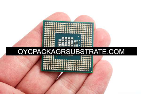
HF Radar PCB Manufacturer
HF Radar PCB Manufacturer,HF Radar PCBs are specialized printed circuit boards designed to support high-frequency radar systems. These PCBs are engineered with materials that offer low dielectric loss and excellent signal propagation characteristics at radar frequencies, typically in the high-frequency (HF) range. HF Radar PCBs facilitate precise signal transmission and reception, crucial for applications such as weather monitoring, aircraft navigation, and defense systems. They are designed to withstand harsh environmental conditions and maintain reliable performance over extended periods. HF Radar PCBs are crucial components in modern radar technology, enabling accurate detection and tracking capabilities in both civil and military applications.
What is an HF Radar PCB?
An HF Radar PCB, or High Frequency Radar PCB, is a specialized type of printed circuit board designed to operate at high frequencies typically used in radar systems. These PCBs are crucial components in radar applications where precision, reliability, and high-performance signal processing are essential.
Key features of HF Radar PCBs include:
- High-Frequency Operation: These PCBs are engineered to handle frequencies typically in the microwave range (GHz), which are necessary for radar systems to accurately detect and process signals.
- Material Selection: They are often constructed using advanced materials with low dielectric constants and losses to minimize signal attenuation and distortion, crucial for maintaining radar sensitivity and accuracy.
- Design Considerations: HF Radar PCBs require meticulous design to ensure controlled impedance, minimal electromagnetic interference (EMI), and efficient heat dissipation to sustain high-performance radar operations.
- Manufacturing Precision: Fabrication techniques for HF Radar PCBs involve high-precision processes to meet stringent tolerances for signal integrity and reliability, ensuring consistent performance in demanding radar environments.
- Applications: These PCBs are integral in various radar systems, including military and aerospace applications for surveillance, navigation, weather monitoring, and other critical tasks where precise and reliable detection capabilities are paramount.
Overall, HF Radar PCBs represent a specialized niche within the broader spectrum of high-frequency electronics, catering specifically to the stringent requirements of radar systems for accuracy, sensitivity, and operational reliability.
HF Radar PCB Manufacturer
What are the HF Radar PCB Design Guidelines?
Designing HF Radar PCBs requires adherence to specific guidelines to ensure optimal performance and reliability in radar applications. Here are key design guidelines:
- Material Selection: Choose PCB materials with low dielectric constant (Dk) and low dissipation factor (Df) to minimize signal loss and ensure stable impedance characteristics at high frequencies.
- Layer Stackup: Design a controlled layer stackup to maintain consistent impedance across different signal layers. Use impedance calculation tools to verify and adjust trace widths and layer thicknesses accordingly.
- Impedance Control: Maintain strict impedance control for high-frequency signal paths. Ensure impedance matching between transmission lines and components to minimize signal reflections and maximize signal integrity.
- Signal Integrity: Minimize cross-talk and electromagnetic interference (EMI) by carefully routing high-frequency traces with adequate spacing and using ground planes effectively to provide shielding and return paths.
- Component Placement: Place critical components, especially RF components and connectors, strategically to minimize parasitic effects and ensure signal integrity. Pay attention to signal routing and avoid sharp bends or discontinuities.
- Power Distribution: Design robust power distribution networks (PDN) with low impedance paths and proper decoupling capacitors near active components to provide clean power and suppress noise.
- Thermal Management: Implement effective thermal management strategies to dissipate heat generated by high-power components or high-frequency operation. Ensure adequate spacing and ventilation around heat-sensitive components.
- Testing and Validation: Perform comprehensive simulations and signal integrity analysis using electromagnetic simulation tools to verify design performance before prototyping. Conduct rigorous testing, including high-frequency testing, to validate PCB functionality and performance.
By following these guidelines, designers can create HF Radar PCBs that meet the stringent requirements of radar systems, ensuring reliable operation, minimal signal degradation, and optimal performance in high-frequency environments.
What is the HF Radar PCB Fabrication Process?
The fabrication process for HF Radar PCBs involves several specialized steps to ensure the PCB meets high-frequency performance requirements. Here’s an overview of the typical fabrication process:
- Material Selection: Choose PCB materials with characteristics suitable for high-frequency operation, such as low dielectric constant (Dk) and low dissipation factor (Df). Common materials include PTFE-based substrates like Rogers RO4000 series or other high-frequency laminates.
- Design Preparation: Use PCB design software to create a detailed layout that adheres to high-frequency design guidelines. This includes careful planning of layer stackup, trace widths, and impedance control structures.
- Preparation of Substrates: Cut and prepare substrate materials according to the design specifications. Ensure cleanliness and smoothness of substrate surfaces to facilitate proper adhesion and etching processes.
- Drilling:Precision drill small-diameter holes for through-hole vias and component mounting pads. Control drill bit tolerances tightly to maintain accuracy and minimize drill wander that could affect signal integrity.
- Lamination: Assemble the layer stackup by laminating prepreg layers and cores together under controlled temperature and pressure. Ensure that copper foil adheres firmly to the substrate to provide reliable electrical connections.
- Etching: Apply a photoresist layer to the copper surface, expose it to UV light through a photo mask that defines the circuit pattern, and develop it to remove unexposed photoresist. Then, etch away exposed copper using an etchant solution to create the circuit traces.
- Plating and Surface Finish: Plate the PCB with copper to increase trace thickness if needed, followed by applying a surface finish like immersion gold or ENIG (Electroless Nickel Immersion Gold) to protect exposed copper and ensure good solderability.
- Silkscreen and Legend Printing: Apply silkscreen printing for component outlines, reference designators, and other markings. Legend printing provides additional information such as component polarity or identification codes.
- Final Inspection: Conduct visual inspection, electrical testing, and possibly impedance testing to ensure the PCB meets design specifications and performance requirements.
- Routing and Profiling: Cut the PCB panels into individual boards using routing or V-scoring methods. Ensure smooth edges and precise dimensions.
- Quality Assurance: Implement quality control measures throughout the process to detect and rectify any defects or deviations from specifications.
By meticulously following these steps, manufacturers can produce HF Radar PCBs that exhibit excellent high-frequency performance, reliability, and durability, meeting the stringent demands of radar system applications.
How do you manufacture an HF Radar PCB?
Manufacturing an HF Radar PCB involves a series of specialized processes designed to ensure high-frequency performance, reliability, and durability essential for radar system applications. Here’s an in-depth look at the manufacturing process:
- Material Selection: The process begins with selecting suitable PCB materials tailored for high-frequency operation. Common choices include PTFE-based laminates such as Rogers RO4000 series or other high-frequency substrates known for their low dielectric constant (Dk) and low dissipation factor (Df). These materials minimize signal loss and maintain stable impedance characteristics at high frequencies.
- Design Preparation: PCB design engineers use specialized CAD software to create a detailed layout according to high-frequency design guidelines. This includes planning the layer stackup, trace widths, and impedance control structures. Design considerations also focus on minimizing signal reflections, cross-talk, and electromagnetic interference (EMI) through strategic component placement and routing.
- Preparation of Substrates:Once the design is finalized, substrate materials are prepared. This involves cutting the laminate sheets to the required dimensions and ensuring cleanliness and smoothness of substrate surfaces. Proper preparation is crucial to facilitate adhesion during the lamination process.
- Layer Stackup: The layer stackup is assembled by laminating alternating layers of prepreg (resin-impregnated fiberglass) and copper-clad laminate cores. This process is conducted under controlled temperature and pressure conditions to ensure proper bonding between layers. The number of layers and their arrangement in the stackup depend on the complexity and functionality required by the radar system.
- Drilling: Precision drilling is performed to create small-diameter holes for through-hole vias and component mounting pads. CNC drilling machines are used to achieve accurate hole placement and size control. The drill bits are chosen carefully to maintain tight tolerances, critical for maintaining signal integrity at high frequencies.
- Plating and Etching: After drilling, the PCB undergoes a series of plating and etching processes. First, a thin layer of copper is electroplated onto the panel surfaces to increase trace thickness and ensure reliable electrical conductivity. Then, a photoresist layer is applied and exposed to UV light through a photomask that defines the circuit pattern. The exposed areas are developed to remove unexposed photoresist, exposing the underlying copper for etching. Chemical etchants are used to selectively remove the exposed copper, leaving behind the desired circuit traces.
- Surface Finish: Once the circuit traces are defined, the PCB undergoes surface finishing processes to protect exposed copper surfaces and ensure good solderability. Common surface finishes for HF Radar PCBs include immersion gold (ENIG), which provides excellent corrosion resistance and solder joint reliability, crucial for high-frequency applications.
- Silkscreen and Legend Printing: Silk screening is applied to print component outlines, reference designators, and other necessary markings on the PCB surface. Legend printing is used to add additional information such as component polarity indicators or identification codes, aiding in assembly and maintenance.
- Quality Assurance:Throughout the manufacturing process, rigorous quality control measures are implemented. Visual inspections, electrical testing, and possibly impedance testing are conducted to verify that the PCB meets design specifications and performance requirements. Any defects or deviations are identified and rectified promptly to ensure product reliability.
- Routing and Profiling: After passing quality checks, the panel is routed or V-scored to separate individual PCBs. Routing involves using CNC machines to cut along the board outline, while V-scoring creates a groove along the board edges for manual separation. Careful attention is given to ensure smooth edges and precise dimensions of the finished PCBs.
- Packaging and Shipping: Once fully assembled and tested, the HF Radar PCBs are packaged according to customer specifications and prepared for shipping. Proper packaging ensures protection during transit to customers or assembly facilities where they will be integrated into radar systems.
By following these comprehensive manufacturing processes and adhering to stringent quality control standards, manufacturers can produce HF Radar PCBs that meet the exacting requirements of high-frequency radar applications. These PCBs are essential components in radar systems used for surveillance, navigation, weather monitoring, and other critical applications where precision and reliability are paramount.
How much should an HF Radar PCB cost?
The cost of an HF Radar PCB can vary widely depending on several factors, including:
- Complexity of Design: The complexity of the PCB design, including the number of layers, intricacy of routing, and special requirements such as controlled impedance, significantly impacts the cost. More complex designs often require more advanced manufacturing techniques and may involve higher material costs.
- Material Selection: The choice of PCB materials plays a crucial role in cost. High-frequency PCB materials such as PTFE-based laminates (e.g., Rogers RO4000 series) or other specialized substrates with low Dk and Df properties are generally more expensive than standard FR4 materials due to their performance characteristics.
- Production Volume: Economies of scale apply in PCB manufacturing. Larger production volumes typically result in lower unit costs due to efficiencies in material usage, setup, and manufacturing processes. Conversely, smaller production runs may incur higher costs per unit.
- Manufacturing Techniques:Advanced manufacturing techniques such as high-precision drilling, fine line etching, and complex layer stackups can increase manufacturing costs. These techniques are often necessary for ensuring high-frequency performance and reliability.
- Surface Finish and Additional Features: The choice of surface finish (e.g., immersion gold, ENIG) and additional features like silk screening, legend printing, and special testing requirements (e.g., impedance testing) can add to the overall cost.
- Supplier and Location:PCB manufacturing costs can also vary based on the supplier’s capabilities, location, and market conditions. Different regions may have different labor costs, overheads, and supply chain dynamics that influence pricing.
As a rough estimate, the cost of an HF Radar PCB for moderate complexity designs and standard production volumes can range from tens to hundreds of dollars per unit. More complex designs or specialized requirements may increase costs significantly. It’s advisable to obtain quotes from several PCB manufacturers to compare pricing based on your specific design and production needs. This allows you to balance cost considerations with the required performance and reliability for your radar system application.
What is an HF Radar PCB base material?
An HF Radar PCB base material refers to the substrate material used in the construction of high-frequency radar printed circuit boards. These materials are chosen for their specific electrical and mechanical properties that are critical for maintaining signal integrity and performance at microwave frequencies typically used in radar systems.
Common base materials for HF Radar PCBs include:
- PTFE-Based Laminates: These are among the most widely used materials for high-frequency applications due to their low dielectric constant (Dk) and low dissipation factor (Df). Examples include materials from the Rogers RO4000 series, such as RO4350B, RO4003C, and RO3003.
- Hybrid Laminates:These laminates combine PTFE with other materials to achieve specific performance characteristics, such as improved thermal conductivity or mechanical strength. An example is the Rogers RO4835 laminate.
- Ceramic-Based Laminates: Ceramic-filled PTFE materials are used for applications requiring higher thermal conductivity and improved dimensional stability. They offer good mechanical strength and reliability under harsh environmental conditions.
- Liquid Crystal Polymer (LCP): LCP materials are known for their excellent electrical properties and dimensional stability at high frequencies. They are suitable for applications demanding high reliability and precision, though less common than PTFE-based materials.
- Other Specialty Materials: Depending on specific design requirements, other materials such as certain polyimides, BT (Bismaleimide Triazine), or cyanate ester resins may be used. These materials offer varying combinations of electrical performance, thermal management, and mechanical strength tailored to specific radar system needs.
The choice of base material for HF Radar PCBs is crucial as it directly impacts key performance metrics such as signal attenuation, impedance stability, and thermal management. Designers select these materials based on the frequency range of operation, power handling capabilities, environmental conditions, and other application-specific requirements to ensure optimal performance and reliability of radar systems.
Which company makes HF Radar PCBs?
Many companies specialize in manufacturing HF Radar PCBs. These companies typically possess advanced technology and specialized manufacturing facilities to meet the stringent requirements of high-frequency operations. They offer a variety of high-frequency PCB material choices, including PTFE-based materials, hybrid materials, ceramic-based materials, and custom solutions tailored to complex designs and high reliability requirements.
For example, Rogers Corporation in the United States is a well-known supplier of high-frequency PCB materials, offering a range of high-performance PTFE-based materials such as the RO4000 series, suitable for manufacturing HF Radar PCBs. Other companies like Isola, Taconic, and Park Electrochemical Corp also have significant influence in the high-frequency PCB market, providing various specialized substrate options and technical support.
Moreover, many specialized PCB manufacturers like Mouser Electronics, Digi-Key Electronics, and Avnet also offer custom manufacturing services for HF Radar PCBs. They collaborate with material suppliers to provide PCB solutions that meet high-frequency requirements for their customers.
Our company is also a manufacturer specializing in high-frequency PCBs. We have advanced manufacturing equipment and an experienced technical team capable of providing high-quality HF Radar PCB products tailored to customer-specific requirements. Our manufacturing process adheres strictly to high-frequency PCB design guidelines to ensure products perform reliably in high-frequency environments, with excellent signal transmission and thermal management capabilities. Whether for single-layer or multi-layer, simple or complex designs, we can customize HF Radar PCB solutions that meet the application needs of our customers.
If you have further inquiries about HF Radar PCBs or would like to learn more about our capabilities and services, please feel free to contact us. We are committed to providing professional support and consultation to meet your needs.
What are the 7 qualities of good customer service?
Good customer service is characterized by several key qualities that contribute to a positive experience for customers. Here are seven important qualities:
- Responsiveness: Customers appreciate prompt responses to their inquiries, concerns, or issues. Effective customer service teams prioritize timely communication and ensure that customers feel heard and valued.
- Empathy:Empathizing with customers’ situations and emotions helps to build rapport and trust. Understanding their perspectives and showing genuine concern for their needs fosters a positive customer service experience.
- Clarity:Providing clear and concise information is essential in customer interactions. Whether explaining products, policies, or solutions to problems, clarity helps to avoid misunderstandings and ensures customers have accurate information.
- Professionalism: Maintaining professionalism in all interactions reflects positively on the company’s image. This includes courteous behavior, respectful language, and a commitment to resolving issues effectively.
- Problem-solving Skills:Effective customer service involves being proactive in addressing and resolving issues. Customer service representatives who are skilled at problem-solving can efficiently identify solutions and follow through to ensure customer satisfaction.
- Personalization: Tailoring interactions to meet the specific needs and preferences of each customer enhances their experience. Personalized service can involve remembering past interactions, addressing customers by name, and offering relevant recommendations.
- Consistency: Consistency in service delivery ensures that customers receive a reliable experience across different interactions and channels. This includes consistency in information provided, response times, and overall service quality.
These qualities collectively contribute to building strong customer relationships and fostering loyalty by demonstrating a commitment to meeting customer expectations and delivering excellent service experiences.
FAQs about HF Radar PCBs
What are HF Radar PCBs?
HF Radar PCBs are printed circuit boards specifically designed to operate at high frequencies, typically in the microwave range. They are used in radar systems for applications such as surveillance, navigation, weather monitoring, and more.
What are the key considerations in designing HF Radar PCBs?
Designing HF Radar PCBs requires attention to factors such as impedance control, signal integrity, thermal management, and material selection (e.g., low Dk and Df materials like PTFE-based laminates) to ensure reliable performance at high frequencies.
Which materials are commonly used for HF Radar PCBs?
Common materials include PTFE-based laminates (e.g., Rogers RO4000 series), hybrid laminates, ceramic-based laminates, and liquid crystal polymers (LCP), chosen for their low dielectric constant (Dk) and low dissipation factor (Df) properties.
What are the manufacturing processes involved in producing HF Radar PCBs?
Manufacturing processes include material preparation, layer stackup, precision drilling for vias and component mounting, etching for circuit pattern definition, surface finishing (e.g., immersion gold), and rigorous quality testing (e.g., impedance testing).
What are the challenges in manufacturing HF Radar PCBs?
Challenges include maintaining precise impedance control, minimizing signal loss and cross-talk, managing thermal dissipation, and ensuring reliability under harsh environmental conditions typical in radar applications.
How can I ensure high reliability and performance of HF Radar PCBs?
Ensure adherence to high-frequency PCB design guidelines, conduct thorough testing (including high-frequency testing and thermal cycling), use quality materials and manufacturing processes, and engage with experienced PCB manufacturers specialized in high-frequency applications.
What are some applications of HF Radar PCBs?
HF Radar PCBs are crucial components in various radar systems used for military and defense applications (e.g., surveillance, target tracking), aerospace (e.g., weather radar), marine navigation, automotive radar systems, and scientific research (e.g., radio astronomy).