
Microtrace LED PCB Manufacturer
We are a professional Microtrace LED PCB Manufacturer, we mainly produce ultra-small gap LED PCBs. and ultrathin Microtrace LED PCB from 3mil to 7mil.
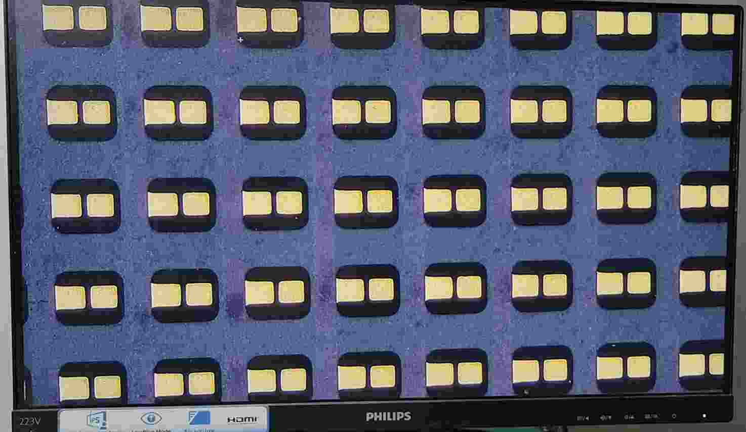
Microtrace LED PCBs are specialized printed circuit boards meticulously engineered for high-performance LED applications. These PCBs boast microscale traces, allowing for intricate routing and high-density LED arrays. The design prioritizes efficient thermal management, crucial for maintaining LED performance and longevity. By utilizing materials with superior thermal conductivity, such as aluminum-core or copper-core substrates, Microtrace LED PCBs effectively dissipate heat, ensuring optimal operation even in demanding environments. Their versatility extends to various applications, including LED lighting fixtures, automotive lighting, display panels, and signage. Designers can customize these PCBs to meet specific project requirements, tailoring layout, trace width, and material selection for optimal performance and reliability. With their precision engineering and advanced thermal management features, Microtrace LED PCBs offer a reliable solution for demanding LED applications, delivering exceptional brightness, efficiency, and longevity.
What is a Microtrace LED PCB?
As of my last update, the term “Microtrace LED PCB” does not specifically refer to a widely recognized or standardized type of PCB (Printed Circuit Board) in the electronics industry. However, I can help clarify some of the terms and concepts that might relate to what you’re asking about:
- Microtrace: This term could refer to the trace widths on a PCB. “Microtrace” might suggest that the PCB uses very fine or narrow traces. Trace widths in PCBs can vary widely depending on the application, with micro-scale traces often used in highly dense or precise electronic applications.
- LED PCB: This refers to a PCB designed specifically for use with LEDs (Light Emitting Diodes). LED PCBs often feature thermal management characteristics since LEDs can generate significant amounts of heat. Common materials used in LED PCBs include metal-core PCBs (MCPCBs), especially aluminum-core, to help with heat dissipation.
Combining these ideas, a “Microtrace LED PCB” could theoretically refer to an LED-specific PCB that features very fine trace widths, possibly for applications requiring high-density LED arrays or precise control over lighting elements in compact devices.
If this is a term from a specific product, technical document, or newer technology development that has emerged after my last training data in December 2023, I recommend checking the most recent sources or product documentation for the most accurate and targeted information.
Microtrace LED PCB
What are Microtrace LED PCB Design Guidelines?
Microtrace LED PCB design guidelines are principles and recommendations aimed at ensuring the optimal performance, reliability, and manufacturability of PCBs specifically designed for LED applications with microscale traces. While these guidelines may vary depending on specific requirements and applications, here are some common considerations:
- Trace Width and Spacing: Ensure that the trace widths and spacing are appropriate for the LED current requirements and thermal management needs. Microscale traces might be necessary to accommodate high-density LED arrays, but they should still provide adequate current carrying capacity and thermal dissipation.
- Thermal Management: Implement effective thermal management techniques to dissipate heat generated by the LEDs. This may involve using metal-core PCBs (MCPCBs), thermal vias, or other heat sinking mechanisms to maintain optimal operating temperatures and prevent premature LED degradation.
- Material Selection: Choose PCB materials with appropriate thermal conductivity, electrical properties, and reliability characteristics. Materials such as aluminum-core or copper-core PCBs are commonly used for LED applications due to their superior thermal performance.
- Component Placement: Carefully position LEDs and other components on the PCB to optimize thermal dissipation, minimize signal interference, and facilitate efficient assembly processes. Proper component placement can also help achieve desired lighting effects and uniformity in LED arrays.
- Electromagnetic Compatibility (EMC): Design the PCB layout to minimize electromagnetic interference (EMI) and ensure compliance with relevant EMC standards. This may involve proper grounding, shielding, and signal routing techniques to prevent signal degradation or interference with nearby electronic devices.
- Manufacturability: Consider manufacturability factors such as solderability, assembly processes, and testability during the PCB design phase. Designing for ease of manufacturing can help reduce production costs and improve overall product quality.
- Testing and Validation: Implement testing procedures to verify the functionality, performance, and reliability of the Microtrace LED PCB design. This may include electrical testing, thermal testing, and accelerated aging tests to ensure compliance with specifications and standards.
These guidelines serve as a starting point for engineers and designers working on Microtrace LED PCBs, but it’s essential to tailor the design approach to specific project requirements and constraints. Collaboration with PCB manufacturers and LED suppliers can also provide valuable insights and expertise to optimize the design for performance and cost-effectiveness.
What is the Microtrace LED PCB Fabrication Process?
The fabrication process for Microtrace LED PCBs follows similar steps to the fabrication of standard PCBs but with additional considerations for the specialized requirements of LED applications and microscale traces. Here’s a general overview of the fabrication process:
- Design and Layout: The process begins with the design and layout of the PCB using CAD (Computer-Aided Design) software. Designers specify the placement of components, trace routing, and any special features required for LED applications, such as thermal vias or heatsinks.
- Material Selection: Select appropriate materials for the PCB based on factors such as thermal conductivity, electrical properties, and reliability. For Microtrace LED PCBs, materials with high thermal conductivity, such as aluminum-core or copper-core substrates, are often preferred to assist with heat dissipation.
- Photolithography: Photolithography is used to transfer the PCB design onto a substrate. A layer of photosensitive material, called photoresist, is applied to the substrate, exposed to UV light through a photomask, and then developed to remove the unexposed areas, leaving behind the desired pattern.
- Etching: The substrate is then subjected to an etching process to remove the exposed copper and create the circuit traces. Chemical etchants, such as ferric chloride or ammonium persulfate, are commonly used to dissolve the copper, leaving behind the patterned traces.
- Drilling: Holes are drilled in the substrate for through-hole components and vias. Microdrilling techniques may be employed to create small-diameter holes for microscale traces and fine-pitch components.
- Plating: A thin layer of metal, typically copper, is electroplated onto the substrate to reinforce the circuit traces and provide a surface for soldering components. Plating may also be used to create surface finishes for improved solderability and corrosion resistance.
- Solder Mask Application: A solder mask is applied to the PCB surface to protect the circuit traces from environmental damage and prevent solder bridges during assembly. The solder mask is typically applied using a screen printing process and cured using UV light.
- Silkscreen Printing: Component designators, logos, and other identifying information are printed onto the PCB surface using a silkscreen printing process. This helps with component placement and assembly.
- Surface Finish: Surface finish is applied to the exposed copper pads to improve solderability and prevent oxidation. Common surface finishes include HASL (Hot Air Solder Leveling), ENIG (Electroless Nickel Immersion Gold), and OSP (Organic Solderability Preservative).
- Quality Control and Testing: The finished PCBs undergo inspection and testing to ensure they meet quality standards and specifications. This may include electrical testing, visual inspection, and dimensional measurements.
- Assembly: Once the PCBs pass inspection, they are ready for component assembly. LEDs and other components are soldered onto the PCB using automated pick-and-place machines and reflow soldering ovens.
- Final Testing and Packaging: The assembled PCBs undergo final testing to verify functionality and performance. Once validated, they are packaged and prepared for shipment to customers or further integration into end products.
Throughout the fabrication process, strict quality control measures are implemented to ensure the reliability and performance of the Microtrace LED PCBs. Collaboration between design engineers, PCB manufacturers, and LED suppliers is essential to optimize the fabrication process for specific project requirements and constraints.
How do you manufacture a Microtrace LED PCB?
Manufacturing a Microtrace LED PCB involves a series of specialized steps to create a printed circuit board with microscale traces optimized for LED applications. Here’s a detailed overview of the manufacturing process:
- Design and Layout: The process starts with the design and layout of the PCB using CAD (Computer-Aided Design) software. Designers specify the placement of components, trace routing, and any special features required for LED applications, such as thermal vias or heatsinks. Careful attention is paid to trace widths, spacing, and thermal management considerations.
- Material Selection: Choose appropriate materials for the PCB based on factors such as thermal conductivity, electrical properties, and reliability. Aluminum-core or copper-core substrates are often preferred for Microtrace LED PCBs due to their superior thermal performance.
- Substrate Preparation: Prepare the substrate material by cleaning and applying a layer of copper foil to one or both sides, depending on the design requirements.
- Photolithography: Use photolithography to transfer the PCB design onto the substrate. A layer of photosensitive material, called photoresist, is applied to the substrate, exposed to UV light through a photomask, and then developed to remove the unexposed areas, leaving behind the desired pattern.
- Etching: Etch away the exposed copper using chemical etchants, such as ferric chloride or ammonium persulfate, to create the circuit traces. This process defines the microscale traces on the PCB.
- Drilling: Drill holes in the substrate for through-hole components and vias. Microdrilling techniques may be used to create small-diameter holes for microscale traces and fine-pitch components.
- Plating: Electroplate a thin layer of metal, typically copper, onto the substrate to reinforce the circuit traces and provide a surface for soldering components. Plating may also be used to create surface finishes for improved solderability and corrosion resistance.
- Solder Mask Application: Apply a solder mask to the PCB surface to protect the circuit traces from environmental damage and prevent solder bridges during assembly. The solder mask is typically applied using a screen printing process and cured using UV light.
- Silkscreen Printing: Print component designators, logos, and other identifying information onto the PCB surface using a silkscreen printing process. This aids in component placement and assembly.
- Surface Finish: Apply a surface finish to the exposed copper pads to improve solderability and prevent oxidation. Common surface finishes include HASL (Hot Air Solder Leveling), ENIG (Electroless Nickel Immersion Gold), and OSP (Organic Solderability Preservative).
- Quality Control and Testing: Inspect the finished PCBs to ensure they meet quality standards and specifications. This may include electrical testing, visual inspection, and dimensional measurements.
- Component Assembly: Once the PCBs pass inspection, proceed with component assembly. LEDs and other components are soldered onto the PCB using automated pick-and-place machines and reflow soldering ovens. Care is taken to align the LED components with the microscale traces and thermal management features.
- Final Testing and Packaging: Conduct final testing to verify functionality and performance. Once validated, the PCBs are packaged and prepared for shipment to customers or further integration into end products.
Throughout the manufacturing process, stringent quality control measures are implemented to ensure the reliability and performance of the Microtrace LED PCBs. Collaboration between design engineers, PCB manufacturers, and LED suppliers is crucial to optimize the manufacturing process for specific project requirements and constraints.
How much should a Microtrace LED PCB cost?
The cost of a Microtrace LED PCB can vary significantly depending on several factors, including the complexity of the design, the size of the board, the number of layers, the materials used, and the quantity ordered. Here are some key factors that can influence the cost:
- Design Complexity: The complexity of the PCB design, including the number of layers, the density of traces, and the presence of special features such as blind vias or controlled impedance, can impact the cost. Microtrace LED PCBs may require intricate routing and thermal management features, which can increase manufacturing costs.
- Material Selection: The choice of materials for the PCB substrate and copper layers can affect the cost. High-performance materials with superior thermal conductivity, such as aluminum-core or copper-core substrates, may be more expensive than standard FR-4 materials.
- Manufacturing Process: Certain manufacturing processes, such as microdrilling for small-diameter holes or precision photolithography for fine traces, may incur additional costs. Specialized processes for thermal management, such as metal-core PCB fabrication, can also impact the overall cost.
- Quantity: Economies of scale typically apply in PCB manufacturing, meaning that larger production quantities often result in lower per-unit costs. Ordering larger quantities of Microtrace LED PCBs can help reduce the cost per board.
- Lead Time:Expedited manufacturing or shorter lead times may come with additional costs. Planning ahead and allowing for longer lead times can help reduce manufacturing costs.
- Additional Services: Optional services such as electrical testing, quality assurance, and component sourcing may add to the overall cost of the PCBs.
Without specific details about the requirements of your Microtrace LED PCB, it’s challenging to provide an exact cost estimate. However, you can obtain quotes from PCB manufacturers by providing them with detailed specifications, including the PCB dimensions, layer count, trace width and spacing requirements, material preferences, and desired quantity. Comparing quotes from multiple suppliers can help you find the best balance between cost, quality, and lead time for your project.
What is Microtrace LED PCB base material?
The base material used for Microtrace LED PCBs can vary depending on specific design requirements and performance criteria. However, some common materials used for Microtrace LED PCBs include:
- Aluminum-Core PCBs (MCPCBs): Aluminum-core PCBs feature a layer of aluminum as the core material, providing excellent thermal conductivity. This makes them well-suited for LED applications where efficient heat dissipation is critical. The aluminum core helps to spread heat away from the LEDs, reducing the risk of overheating and extending the lifespan of the LEDs.
- Copper-Core PCBs: Similar to aluminum-core PCBs, copper-core PCBs feature a copper layer as the core material. Copper is also an excellent conductor of heat, making copper-core PCBs effective for LED applications requiring efficient thermal management. Copper-core PCBs may offer even better thermal performance compared to aluminum-core PCBs but may be more expensive.
- FR-4 with Thermal Management Features: FR-4 is a standard substrate material used in PCB manufacturing due to its affordability and versatility. For Microtrace LED PCBs, FR-4 substrates with additional thermal management features, such as thermally conductive fillers or metal backings, may be used to enhance heat dissipation.
- Ceramic Substrates: Ceramic substrates offer excellent thermal conductivity and mechanical stability, making them suitable for high-power LED applications. Ceramic substrates can withstand high operating temperatures and provide reliable performance in demanding environments.
- Metal Substrates: Other metal substrates, such as copper or steel, may also be used for Microtrace LED PCBs, particularly in applications requiring superior thermal performance or ruggedness.
The choice of base material for Microtrace LED PCBs depends on factors such as thermal requirements, cost constraints, and performance specifications. Designers typically evaluate these factors and select the most appropriate material to ensure optimal performance and reliability for the specific LED application.
Which company makes Microtrace LED PCBs?
Currently, there are many companies specialized in manufacturing Microtrace LED PCBs, including OSRAM, Nichia Corporation, Cree, Seoul Semiconductor, and others. These companies have rich experience and technical expertise in the field of LED lighting, and they are capable of providing various types of LED PCBs, including Microtrace LED PCBs.
For our company, if we have the relevant manufacturing and technological capabilities, then we can also produce Microtrace LED PCBs. As a professional PCB manufacturer, we have advanced production equipment and a skilled technical team to meet the diverse needs of customers. Our manufacturing process and technological capabilities ensure the production of high-quality and highly reliable Microtrace LED PCBs.
Firstly, our engineering team has extensive experience in PCB design and layout, capable of designing PCB layouts that meet the standards of Microtrace LED PCBs based on customer specifications and requirements. We use advanced CAD software for design and simulation to ensure feasibility and performance optimization.
Secondly, we have advanced manufacturing equipment and processes that enable us to achieve micro-scale tracing during the PCB manufacturing process to meet the requirements of Microtrace LED PCBs. We employ precise photolithography and etching techniques to ensure that the trace widths and spacing on the PCB meet specifications and achieve high-precision hole drilling.
Additionally, our quality control system is rigorous, ensuring that the produced Microtrace LED PCBs meet customer requirements and standards. We conduct thorough inspections and testing, including visual inspection, electrical testing, and thermal performance testing, to ensure consistent quality and reliability for each PCB.
In conclusion, as a PCB manufacturer with extensive experience and technological capabilities, we have the ability to produce high-quality Microtrace LED PCBs and can customize various specifications and designs according to customer requirements. We are committed to providing reliable solutions to customers and playing an important role in the development of the LED lighting industry.
What are the 7 qualities of good customer service?
Good customer service is characterized by several key qualities that help build positive relationships with customers and ensure their satisfaction. Here are seven essential qualities of good customer service:
- Responsiveness: Good customer service involves being prompt and responsive to customer inquiries, requests, and concerns. Customers appreciate quick responses to their questions or issues, whether it’s through email, phone, or live chat support.
- Empathy: Empathy is the ability to understand and relate to the feelings and perspectives of customers. Good customer service representatives listen actively to customers, validate their concerns, and demonstrate genuine empathy to build trust and rapport.
- Clarity and Communication Skills: Effective communication is crucial in providing good customer service. Customer service representatives should communicate clearly and concisely, using language that is easy for customers to understand. They should also be able to articulate solutions or explanations effectively.
- Problem-Solving Skills: Good customer service involves being proactive in addressing customer problems and finding solutions to their issues. Customer service representatives should have strong problem-solving skills, be resourceful, and take initiative to resolve customer concerns promptly.
- Professionalism: Professionalism is essential in all interactions with customers. Customer service representatives should maintain a courteous and respectful demeanor, even in challenging situations. They should also adhere to company policies and procedures while assisting customers.
- Product Knowledge: Having a deep understanding of the products or services offered is critical for providing good customer service. Customer service representatives should be knowledgeable about the features, benefits, and usage of the products or services to address customer inquiries effectively.
- Follow-Up and Feedback: Good customer service extends beyond the initial interaction. Following up with customers to ensure their satisfaction and gather feedback is crucial for building long-term relationships. Customer service representatives should seek feedback, address any remaining concerns, and thank customers for their business.
By embodying these qualities, businesses can deliver exceptional customer service experiences that leave a lasting positive impression on customers and contribute to customer loyalty and retention.
FAQs (Frequently Asked Questions)
What are Microtrace LED PCBs?
Microtrace LED PCBs are printed circuit boards specifically designed for LED applications, featuring microscale traces optimized for high-density LED arrays and efficient thermal management.
What are the benefits of using Microtrace LED PCBs?
Microtrace LED PCBs offer several advantages, including enhanced thermal conductivity, improved heat dissipation, higher LED density, and precise control over lighting elements, resulting in better performance and reliability for LED applications.
How are Microtrace LED PCBs different from standard LED PCBs?
Microtrace LED PCBs feature narrower trace widths and smaller spacing between traces compared to standard LED PCBs, allowing for higher density LED arrays and more efficient heat dissipation. They are specifically optimized for micro-scale LED applications.
What are some common applications of Microtrace LED PCBs?
Microtrace LED PCBs are used in a wide range of applications, including LED lighting fixtures, display panels, automotive lighting, signage, and backlighting for LCD screens. They are particularly beneficial in applications where space is limited, and high brightness and efficiency are required.
How are Microtrace LED PCBs manufactured?
The manufacturing process for Microtrace LED PCBs involves specialized techniques such as precise photolithography, microscale tracing, and thermal management features. These PCBs are typically fabricated using materials with high thermal conductivity, such as aluminum-core or copper-core substrates.
What factors should be considered when designing Microtrace LED PCBs?
Design considerations for Microtrace LED PCBs include thermal management, trace width and spacing, component placement, material selection, and manufacturability. These factors are critical for optimizing performance, reliability, and efficiency.
Can Microtrace LED PCBs be customized for specific applications?
Yes, Microtrace LED PCBs can be customized to meet the specific requirements of different LED applications. Designers can tailor the PCB layout, thermal management features, and material selection to optimize performance and functionality for a particular application.
What are the cost considerations for Microtrace LED PCBs?
The cost of Microtrace LED PCBs depends on factors such as design complexity, material selection, manufacturing processes, and quantity ordered. Generally, higher complexity and customization may result in higher costs, while larger production quantities may lower the cost per unit.