
Semiconductor FC BGA substrate Manufacturer. The best samllest bump pitch with 100um, the best smallest trace are 9um. and the smallest gap are 9um. most of the design are 9um to 25um trace and spacing.
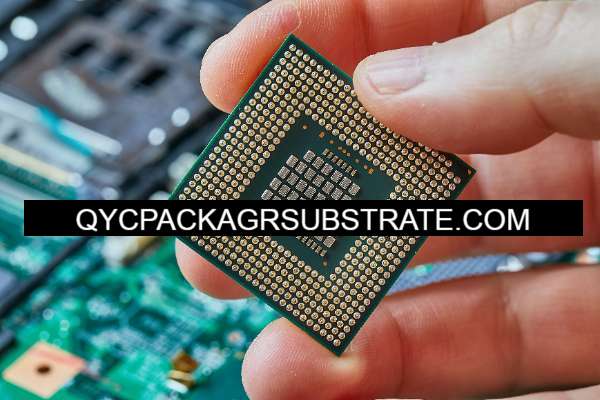
The FC BGA substrate is a crucial intermediary in semiconductor packaging, forming a reliable electrical and mechanical connection between integrated circuits and printed circuit boards through its fine-pitch ball grid array configuration with closely arranged solder balls.
This design features a high-density arrangement of interconnects, enabling the packaging of advanced and high-performance semiconductor devices. The closely spaced solder balls contribute to the reliability of the connection, making the FC BGA substrate a key component in the successful integration of ICs into electronic systems.
Diverse types of FC BGA substrates, including single-layer and multi-layer variations, cater to specific performance requirements and applications. Within the realm of IC packaging, the FC BGA substrate significantly shapes signal integrity, thermal management, and overall electrical performance.
In contrast to traditional PCBs, FC BGA substrates are meticulously crafted for semiconductor packaging, exhibiting distinctions in materials, design intricacies, and manufacturing processes. While traditional PCBs find application in a broader electronic context, FC BGA substrates are specialized to address the challenges posed by densely packed and high-performance ICs.
The structure of FC BGA substrates typically encompasses layers of dielectric material, conductive traces, solder mask, and solder balls arranged in a fine-pitch grid on the underside. Manufacturing technologies involve precise techniques such as laser drilling, electroplating, and solder ball attachment to guarantee the reliability and performance of the end product.
In summary, FC BGA substrates play a pivotal role in semiconductor technology by bridging the gap between ICs and PCBs. Their fine-pitch design, diverse types, and specialized manufacturing processes collectively contribute to enhancing the efficiency and reliability of contemporary electronic systems.
What Functions Does FC BGA Substrate Serve?
The FC BGA (Fine-pitch Ball Grid Array) substrate transcends its fundamental role as a physical support platform, emerging as a crucial medium for electrical connectivity and thermal management within semiconductor packaging. In contrast to conventional support structures, its fine-pitch ball grid array configuration is intricately crafted to facilitate dense and efficient electrical connections between integrated circuits (ICs) and printed circuit boards (PCBs). This meticulous design precision not only accommodates the needs of intricate and high-performance semiconductor devices but also guarantees optimal signal transmission.
In addition to its electrical connectivity function, the FC BGA substrate plays a pivotal role in addressing thermal challenges. As electronic devices advance in power and complexity, effective heat dissipation becomes crucial. The FC BGA substrate’s design incorporates features that facilitate efficient heat dissipation, preventing overheating and contributing to the prolonged stability of device operation. This dual functionality sets it apart, as it not only ensures reliable electrical connections but also actively manages the thermal environment to enhance overall system performance.
In summary, the FC BGA substrate distinguishes itself by serving as a versatile component that not only provides essential physical support but also acts as a critical enabler for both electrical and thermal aspects within semiconductor packaging. Its precise design enhances signal transmission and thermal regulation, contributing to the sustained functionality and longevity of sophisticated electronic systems.
What Are the Different Types of FC BGA Substrate?
FC BGA (Fine-pitch Ball Grid Array) substrates encompass a range of types, each strategically crafted to meet distinct application scenarios in the semiconductor industry. This diversity in substrate types allows for specialized solutions tailored to specific needs within semiconductor applications.
Single-Layer FC BGA Substrates:
Advantages:Single-layer FC BGA substrates feature a straightforward design and manufacturing process, providing cost-effective solutions tailored for semiconductor applications of lower complexity.
Characteristics: These substrates consist of a single layer of dielectric material with conductive traces, making them suitable for applications where a lower level of complexity is acceptable.
Multi-Layer FC BGA Substrates:
Advantages: Multi-layer FC BGA substrates provide enhanced performance for complex semiconductor devices by offering multiple layers of dielectric material and conductive traces.
Characteristics: The multi-layer design allows for more sophisticated routing of traces, accommodating the intricate interconnectivity requirements of high-performance integrated circuits.
High-Frequency FC BGA Substrates:
Advantages: High-frequency FC BGA substrates are optimized for applications where signal integrity at elevated frequencies is crucial, such as in high-speed data communication or RF (Radio Frequency) devices.
Characteristics: These substrates may feature specialized materials and design considerations to minimize signal loss and maintain signal integrity at higher frequencies.
Thermal Management FC BGA Substrates:
Advantages: Crafted for effective thermal management, these substrates are intricately designed to efficiently dissipate the heat generated by semiconductor devices, ensuring optimal operational temperatures.
Characteristics: They may incorporate elements such as heat sinks, thermal vias, or specific materials with enhanced thermal conductivity to address the thermal challenges presented by high-power semiconductor applications.
Embedded Passive FC BGA Substrates:
Benefits: Embedded passive FC BGA substrates seamlessly integrate passive components (resistors, capacitors, inductors) directly into the substrate, reducing the reliance on external discrete components.
Features: This substrate type enhances miniaturization, diminishes parasitic effects, and enhances overall performance in applications where space constraints are critical.
In summary, the diverse types of FC BGA substrates cater to a wide range of semiconductor applications, offering tailored solutions to meet specific performance and design requirements. Whether focusing on simplicity, high frequency, thermal considerations, or embedded passives, each type serves a unique role in enhancing the efficiency and functionality of semiconductor devices.
How Does FC BGA Substrate Relate to IC Packaging?
The FC BGA (Flip Chip Ball Grid Array) substrate is a crucial component in the intricate process of packaging integrated circuits (ICs). IC packaging involves enclosing semiconductor devices to shield them from external elements, offer structural support, and establish essential electrical connections with the external environment.
Specifically tailored for flip chip packaging, a widely adopted IC assembly method, the FC BGA substrate assumes a central role. In flip chip configuration, the semiconductor die is inverted, and its active surface is directly affixed to the substrate via solder bumps. These solder bumps serve as electrical conduits, efficiently transmitting signals.
The FC BGA substrate fulfills several pivotal functions:
Electrical Conduction: The substrate establishes intricate electrical pathways, connecting the solder bumps on the flip-chipped die to the external leads of the package. This enables the seamless transmission of signals between the integrated circuit and the broader electronic system.
Thermal Management: Acknowledging the heat generated during electronic device operation, the FC BGA substrate is designed to dissipate this heat from the semiconductor die. This ensures the maintenance of optimal operating temperatures, preventing overheating and potential performance issues.
Structural Support: Functioning as a robust foundation, the substrate provides stability, safeguarding the fragile semiconductor components from mechanical stresses, including bending and flexing.
Signal Integrity: The design of the FC BGA substrate is meticulously crafted to preserve signal integrity. By minimizing signal loss and mitigating crosstalk, it ensures the reliability of signal transmission between the IC and the external environment.
Form Factor and Size Optimization: In the context of electronic devices shrinking in size, the FC BGA substrate contributes significantly to the overall size and form factor of the IC package. Its design and material properties are carefully considered to meet evolving size constraints.
In summary, the FC BGA substrate stands as a critical enabler in the IC packaging process. By facilitating electrical connections, providing structural support, managing thermal considerations, and contributing to the overall efficiency and reliability of integrated circuits, it plays a pivotal role in diverse electronic applications.
How Does FC BGA Substrate Differ from Traditional PCBs?
FC BGA (Flip-Chip Ball Grid Array) substrates represent a departure from conventional PCB (Printed Circuit Board) technologies, introducing innovations in materials and design that significantly impact electronic device performance and form factor.
Substrate Material:
Traditional PCBs: Predominantly employ FR-4, a common substrate material.
FC BGA Substrate: Utilizes advanced materials like BT, delivering superior thermal and electrical characteristics crucial for high-performance applications.
Flip-Chip Technology:
Traditional PCBs: Utilize traditional mounting methods, such as through-hole or surface mount technology.
FC BGA Substrate: Features flip-chip technology, wherein the chip is inverted and directly connected to the substrate. This reduces signal path lengths, enhancing overall performance.
Interconnection Technology:
Traditional PCBs: Rely on wire bonding or soldering for interconnections.
FC BGA Substrate: Employs solder balls, ensuring robust connections that contribute to improved electrical reliability.
High-Density Interconnect (HDI) Technology:
Traditional PCBs: Limited in HDI capabilities.
FC BGA Substrate: Embraces HDI technology with fine lines and smaller vias, enabling increased component density and superior signal integrity.
Substrate-Like PCB (SLP):
Traditional PCBs: SLP is not a standard term in traditional designs.
FC BGA Substrate: Often referred to as SLP due to its slim and compact nature, optimizing space utilization and supporting device miniaturization.
Motherboard Design:
Traditional PCBs: Conventional PCB technology is prevalent.
FC BGA Substrate: Facilitates more efficient and compact motherboard designs, essential for the development of smaller electronic devices.
Advantages of FC BGA Substrate:
Size and Weight Reduction: FC BGA enables a more streamlined design, reducing the overall dimensions and weight of electronic devices.
Enhanced Electrical Performance: The flip-chip design and advanced materials contribute to improved electrical performance and signal integrity.
Optimized Thermal Management: Superior thermal properties of FC BGA substrate materials enhance heat dissipation, addressing thermal challenges in high-performance applications.
In essence, FC BGA substrates offer a sophisticated alternative to traditional PCBs, showcasing advancements that enhance electrical performance, enable miniaturization, and improve thermal management in electronic device design.
What Is the Main Structure and What Are the Manufacturing Technologies of FC BGA Substrate?
The primary architecture of an FC BGA (Flip-Chip Ball Grid Array) substrate is meticulously crafted to maximize the synergy between the semiconductor chip and the printed circuit board (PCB). This intricate design is pivotal for achieving superior electrical performance, reducing signal path lengths, and enabling effective thermal management within electronic devices.
Base Material:
At the core of the structure lies an advanced base material, often composed of materials like Bismaleimide Triazine (BT). This choice ensures exceptional thermal stability, a low dielectric constant, and robust mechanical properties, forming a solid foundation for the substrate.
Build-Up Layers:
Multiple layers, known as build-up layers, are incorporated into the structure to facilitate high-density interconnects. These layers play a crucial role in efficiently routing signals through the intricate circuitry of the electronic device.
Copper Traces and Vias:
Copper traces weave across the substrate, forming the conductive pathways necessary for the seamless flow of electrical signals. Vias, which connect different layers vertically, contribute to the intricate network of the substrate, supporting efficient signal propagation.
Solder Mask:
A protective layer of solder mask is applied over the copper traces. This not only shields against unintended electrical connections but also enhances the overall durability of the substrate.
Solder Balls:
Placed strategically on the substrate, solder balls serve as pivotal connection points between the semiconductor chip and the board. This is a fundamental aspect of the flip-chip technology employed in FC BGA, promoting improved electrical connections.
The manufacturing processes associated with FC BGA substrates leverage advanced technologies such as High-Density Interconnect (HDI) and improved semi-additive methods. These innovations contribute to finer feature resolution, enabling the creation of intricate circuit patterns that align with the demands of modern electronics.
In essence, the intricately designed structure of FC BGA substrates represents a harmonious integration of materials and features, optimizing the connection between semiconductor components and the PCB. This results in enhanced electrical efficiency, minimized signal path lengths, and effective thermal management—qualities that are pivotal in meeting the evolving demands of high-performance electronic devices.
What Are Frequently Asked Questions (FAQs) about FC BGA Substrate?
How does FC BGA differ from traditional PCBs?
FC BGA utilizes advanced materials, flip-chip technology, and high-density interconnects, resulting in superior electrical performance and enabling more compact designs compared to traditional PCBs.
What is High-Density Interconnect (HDI) technology in FC BGA substrates?
HDI technology involves fine lines and smaller vias, enabling increased component density and improved signal integrity within FC BGA substrates.
What advantages does FC BGA offer in terms of thermal management?
FC BGA substrates often incorporate materials with superior thermal properties, facilitating efficient heat dissipation and contributing to enhanced thermal management in electronic devices.
How does the manufacturing process of FC BGA substrates differ from traditional PCBs?
FC BGA manufacturing involves advanced processes like High-Density Interconnect (HDI) and improved semi-additive methods, achieving finer feature resolution and intricate circuit patterns compared to traditional PCBs.
What Is the Conclusion Regarding FC BGA Substrate’s Role in the Semiconductor Industry?
In conclusion, the FC BGA (Flip-Chip Ball Grid Array) substrate stands as a pivotal force in the semiconductor industry, playing an irreplaceable role in advancing electronic technology. Its innovative design, utilizing flip-chip technology, advanced materials, and high-density interconnects, significantly enhances the performance and miniaturization of electronic devices. FC BGA substrates are instrumental in addressing the ever-increasing demands for compactness, improved thermal management, and superior electrical efficiency. As a cornerstone in semiconductor packaging, FC BGA substrates continue to drive innovation, pushing the boundaries of what is achievable in the electronic landscape. Their integration remains indispensable for powering the next generation of high-performance and compact electronic devices.