
Ceramic PCB substrates Manufacturing. Ceramic series materials. Such as:96AL2O3 Ceramic, ALN Ceramic, and other Ceramic base materials. We have made the Ceramic materials PCBs, and samll BGA Ceramic package Substrates from 2 layer to 20 layers.
Ceramic PCB substrates are a type of printed circuit board (PCB) that utilizes ceramic materials as the base. These substrates offer exceptional thermal conductivity, electrical insulation, and mechanical stability compared to traditional organic substrates. Due to their excellent properties, ceramic PCB substrates are commonly used in high-power and high-frequency electronic applications where thermal management is critical. The ceramic material used, such as alumina (Al2O3) or aluminum nitride (AlN), provides excellent heat dissipation, making them ideal for devices operating in harsh environments or those requiring precise temperature control. Additionally, ceramic PCB substrates exhibit low dielectric loss and high dielectric strength, ensuring reliable performance in demanding conditions. Their ability to withstand extreme temperatures, corrosive chemicals, and high voltages makes them suitable for various industries, including aerospace, automotive, telecommunications, and power electronics. Overall, ceramic PCB substrates play a crucial role in advancing technology by enabling the development of robust and efficient electronic devices.
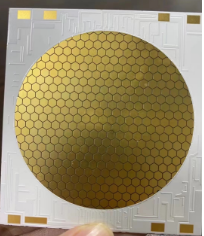
Ceramic PCB
What is a Ceramic PCB Substrate?
Ceramic PCB Substrates manufacturing.High speed and high frequency material packaging substrate manufacturing. Advanced packaging substrate production process and technology
A Ceramic PCB (Printed Circuit Board) substrate is a type of substrate used in electronic devices for mounting and interconnecting electronic components. Unlike traditional PCB substrates such as FR-4 (a type of epoxy-based fiberglass material), ceramic PCB substrates are made of ceramic materials.
Ceramic PCB substrates offer several advantages over traditional substrates, including:
- High Thermal Conductivity: Ceramic materials have high thermal conductivity compared to traditional PCB substrates, which helps in dissipating heat generated by electronic components more efficiently. This is particularly beneficial in high-power applications where thermal management is critical.
- High Electrical Insulation: Ceramic materials exhibit excellent electrical insulation properties, which prevent leakage of current between conductive traces and ensure reliable performance of electronic circuits.
- High Mechanical Strength: Ceramic PCB substrates are mechanically robust and can withstand harsh operating conditions, making them suitable for use in rugged environments and applications where mechanical stress is a concern.
- Chemical Resistance: Ceramic materials are often resistant to chemicals and environmental factors, providing protection against corrosion and other forms of degradation.
- Miniaturization: Ceramic PCB substrates can be manufactured with very fine features, enabling the miniaturization of electronic devices and increasing the packing density of components on the board.
Common ceramic materials used for PCB substrates include alumina (Al2O3), aluminum nitride (AlN), and silicon carbide (SiC). These materials can be tailored to specific requirements such as thermal conductivity, coefficient of thermal expansion (CTE), and dielectric properties, making them suitable for a wide range of applications in industries such as automotive, aerospace, telecommunications, and power electronics.
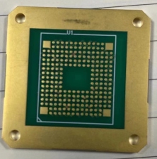
BGA Ceramic Substrate
What are the Ceramic PCB Design Guidelines?
The design guidelines for ceramic PCB typically include the following aspects:
- Material Selection: Choose ceramic materials suitable for specific application requirements, such as alumina, aluminum nitride, or silicon carbide. Consider material properties like thermal conductivity, dielectric constant, and mechanical strength.
- Layer Thickness and Dimensions: Determine the layer thickness and dimensions of the PCB, usually considering thermal management, mechanical strength, and component layout.
- Routing Design: Perform rational routing design considering signal integrity, electrical performance, and thermal conduction requirements. Avoid sharp corners and narrow traces to reduce mechanical stress and thermal strain.
- Heat Dissipation Design: Ensure effective heat dissipation design by employing appropriate heat dissipation structures, heat-dissipating devices, and thermal paths to lower temperatures and prevent component overheating.
- Package Selection: Choose suitable packaging types for ceramic PCB, such as surface-mount packaging (SMT) or through-hole packaging, based on design requirements and production processes.
- Electrical Performance Optimization: Optimize the electrical performance of the PCB, including reducing signal transmission losses, improving anti-interference capability, and minimizing electrical noise.
- Separation of Analog and Digital Signals: Properly separate and isolate analog and digital signals to reduce interference and improve signal quality.
- Special Process Considerations: Consider special process requirements during ceramic PCB manufacturing, such as casting, drilling, and surface treatment.
- Environmental Adaptability: Consider the adaptability of the PCB to different environmental conditions, including temperature, humidity, vibration, and corrosion.
- Reliability Analysis: Conduct reliability analysis and testing to validate the design’s reliability and stability under various conditions, ensuring that the product meets required lifespan and performance standards.
These design guidelines help ensure that ceramic PCB designs meet the requirements of specific applications and maintain good performance and reliability during production and use.
What is the Ceramic PCB Fabrication Process?
The fabrication process for ceramic PCBs typically involves several steps, which may vary slightly depending on the specific requirements of the design and the manufacturing capabilities of the facility. Here’s an overview of the typical ceramic PCB fabrication process:
- Design Preparation: The process begins with the preparation of the PCB design layout using computer-aided design (CAD) software. This layout defines the arrangement of conductive traces, vias, pads, and components on the ceramic substrate.
- Substrate Preparation: The ceramic substrate material, such as alumina (Al2O3), aluminum nitride (AlN), or silicon carbide (SiC), is prepared in the desired size and thickness. The substrate may undergo surface treatment processes to improve adhesion and facilitate subsequent fabrication steps.
- Conductor Deposition: Conductive traces are formed on the ceramic substrate using techniques such as thick film screen printing, thin film deposition (sputtering or evaporation), or laser direct structuring (LDS). These traces define the electrical pathways on the PCB.
- Via Formation: Vias, which are holes that establish electrical connections between different layers of the PCB, are created using drilling or laser ablation techniques. These vias may be filled with conductive material to enhance electrical conductivity.
- Component Attachment: Surface-mounted components (SMD) or through-hole components are attached to the ceramic substrate using soldering or adhesive bonding processes. Precision placement equipment ensures accurate positioning of components according to the PCB design.
- Insulating Layer Deposition: Insulating layers, often made of dielectric materials such as glass or ceramic, are deposited or laminated onto the substrate to provide electrical insulation between conductive traces and components.
- Surface Finishing: Surface finishing processes, such as solder mask application and surface plating (e.g., gold or tin), are performed to protect exposed conductive traces, facilitate soldering, and improve the PCB’s durability and reliability.
- Testing and Inspection: The fabricated ceramic PCB undergoes rigorous testing and inspection procedures to verify electrical continuity, insulation integrity, dimensional accuracy, and overall functionality. This may include electrical testing, visual inspection, and automated optical inspection (AOI).
- Final Assembly: If necessary, additional assembly steps such as attaching heat sinks, connectors, or protective enclosures may be performed to complete the ceramic PCB assembly.
- Quality Assurance and Packaging: The finished ceramic PCBs undergo final quality assurance checks to ensure compliance with specifications and customer requirements. They are then packaged and prepared for shipment to customers or further integration into electronic devices.
Throughout the fabrication process, strict quality control measures are implemented to ensure consistency, reliability, and adherence to industry standards and customer specifications. Collaboration between design engineers, manufacturing specialists, and quality assurance personnel is essential to optimize the fabrication process and deliver high-quality ceramic PCBs.
How do you manufacture a Ceramic PCB?
Manufacturing a ceramic PCB involves a series of steps that require specialized equipment and expertise. Here’s a general overview of the manufacturing process for ceramic PCBs:
- Design Preparation: The manufacturing process begins with the preparation of the PCB design using computer-aided design (CAD) software. This design specifies the layout of conductive traces, vias, pads, and components on the ceramic substrate.
- Substrate Selection and Preparation: Choose the appropriate ceramic material for the PCB substrate based on the desired properties such as thermal conductivity, dielectric constant, and mechanical strength. The ceramic substrate is prepared by cutting it into the desired shape and size.
- Conductor Deposition: Conductive traces are formed on the ceramic substrate using one of several techniques:
– Thick Film Printing: Conductive paste is screen-printed onto the substrate using a stencil, and then fired in a kiln to sinter the conductive material onto the surface.
– Thin Film Deposition: Metal films are deposited onto the substrate using techniques such as sputtering or evaporation. These films are then patterned using photolithography and etching processes to create the conductive traces.
– Laser Direct Structuring (LDS): A laser is used to selectively activate areas of the substrate, allowing for the deposition of a conductive material onto those activated areas.
- Via Formation: Vias, which establish electrical connections between different layers of the PCB, are created using drilling or laser ablation techniques. These vias may be filled with conductive material to enhance electrical conductivity.
- Component Attachment: Surface-mounted components (SMD) or through-hole components are attached to the ceramic substrate using soldering or adhesive bonding processes. Precision placement equipment ensures accurate positioning of components according to the PCB design.
- Insulating Layer Deposition: Insulating layers, often made of dielectric materials such as glass or ceramic, are deposited or laminated onto the substrate to provide electrical insulation between conductive traces and components.
- Surface Finishing: Surface finishing processes such as solder mask application and surface plating (e.g., gold or tin) are performed to protect exposed conductive traces, facilitate soldering, and improve the PCB’s durability and reliability.
- Testing and Inspection: The manufactured ceramic PCB undergoes rigorous testing and inspection procedures to verify electrical continuity, insulation integrity, dimensional accuracy, and overall functionality. This may include electrical testing, visual inspection, and automated optical inspection (AOI).
- Final Assembly and Packaging: If necessary, additional assembly steps such as attaching heat sinks, connectors, or protective enclosures may be performed to complete the ceramic PCB assembly. The finished PCBs are then packaged and prepared for shipment to customers or further integration into electronic devices.
Throughout the manufacturing process, strict quality control measures are implemented to ensure consistency, reliability, and adherence to industry standards and customer specifications. Collaboration between design engineers, manufacturing specialists, and quality assurance personnel is essential to optimize the manufacturing process and deliver high-quality ceramic PCBs.
How much should a Ceramic PCB cost?
The cost of a ceramic PCB can vary widely depending on several factors, including the complexity of the design, the choice of ceramic material, the manufacturing processes involved, the quantity ordered, and the supplier or manufacturer’s pricing structure. Generally, ceramic PCBs tend to be more expensive than traditional FR-4 PCBs due to the specialized materials and manufacturing techniques involved. Here are some key factors that can influence the cost of ceramic PCBs:
- Design Complexity: The complexity of the PCB design, including the number of layers, the density of components, and the intricacy of the routing, can significantly impact the cost. More complex designs require more time and resources to manufacture, which may result in higher costs.
- Ceramic Material: The choice of ceramic material for the substrate can affect the cost. Different ceramic materials have varying properties and manufacturing requirements, which can influence the overall cost of production.
- Manufacturing Processes: The manufacturing processes used to create the ceramic PCB, such as thick film printing, thin film deposition, laser processing, and via formation techniques, can impact the cost. Some processes may be more time-consuming or require specialized equipment, resulting in higher production costs.
- Order Quantity: The quantity of ceramic PCBs ordered can affect the unit cost. Larger production runs typically result in lower unit costs due to economies of scale, while smaller quantities may incur higher costs per unit.
- Additional Services: Additional services such as testing, inspection, surface finishing, and assembly can add to the overall cost of ceramic PCB production.
- Supplier and Location: The choice of supplier or manufacturer and their location can also influence the cost. Different suppliers may offer varying pricing structures, and factors such as labor costs and overhead expenses can vary depending on the manufacturing location.
To get an accurate estimate of the cost of ceramic PCBs for a specific project, it’s essential to consult with multiple suppliers or manufacturers, provide detailed specifications of the PCB design, and consider factors such as order quantity, lead time, and additional services required.
What is Ceramic PCB Base Material?
The ceramic PCB base material refers to the substrate on which the electronic components and conductive traces are mounted and interconnected to create a printed circuit board (PCB). Ceramic PCBs are composed of a ceramic material serving as the base or substrate, onto which conductive traces are applied to form the circuitry. The choice of ceramic material for the base is crucial as it affects the PCB’s thermal, mechanical, and electrical properties. Common ceramic materials used as base materials for ceramic PCBs include:
- Alumina (Al2O3): Alumina is one of the most widely used ceramic materials for PCB substrates. It offers excellent thermal conductivity, high mechanical strength, and good electrical insulation properties. Alumina-based ceramic PCBs are suitable for high-power applications and harsh environments.
- Aluminum Nitride (AlN): Aluminum nitride is valued for its exceptionally high thermal conductivity, making it an excellent choice for applications requiring efficient heat dissipation. AlN-based ceramic PCBs are commonly used in high-power electronic devices, LEDs, and microwave applications.
- Silicon Carbide (SiC): Silicon carbide is known for its high thermal conductivity, excellent mechanical strength, and resistance to temperature extremes and chemical corrosion. SiC-based ceramic PCBs are used in demanding applications such as power electronics, aerospace, and automotive industries.
- Beryllium Oxide (BeO): Beryllium oxide offers exceptional thermal conductivity, low dielectric constant, and good mechanical properties. However, BeO is less commonly used due to health and safety concerns associated with beryllium exposure.
These ceramic materials provide advantages over traditional organic substrates (e.g., FR-4) in terms of thermal performance, reliability, and durability. The choice of ceramic base material depends on the specific requirements of the application, including thermal management needs, operating environment, and electrical performance criteria.
Which company makes Ceramic PCBs?
There are many companies that produce Ceramic PCBs (Printed Circuit Boards), with some well-known manufacturers including Ceramic Substrates, CRRC (China South Locomotive and Rolling Stock Corporation), Kyocera, LG Innotek, and others. These companies have rich experience and advanced manufacturing technologies in the field of ceramic PCBs, providing high-quality products and customized solutions for various industries.
In our company, we are also a professional manufacturer of Ceramic PCBs. We have advanced production equipment and a skilled technical team, offering the following advantages and services:
- Rich Experience: We have years of experience in manufacturing Ceramic PCBs, with in-depth knowledge of various ceramic materials and manufacturing processes.
- Customized Solutions: We can provide customized Ceramic PCB solutions based on the specific requirements of our customers, including design, material selection, and process optimization.
- High-Quality Products: We strictly control the quality during the production process, utilizing advanced testing equipment and processes to ensure that our products meet international standards and customer requirements.
- Timely Delivery: We are capable of providing fast and on-time delivery services according to customer needs, ensuring that projects are completed and delivered on schedule.
- Technical Support: Our technical team can offer professional technical support and consulting services to help address any issues or challenges related to Ceramic PCBs.
In summary, as a professional Ceramic PCB manufacturer, we are committed to providing customers with high-quality, customized products and services to meet their needs and achieve mutual development.
What are the 7 Qualities of Good Customer Service?
Good customer service is essential for building strong relationships with customers and ensuring their satisfaction. Here are seven qualities that characterize good customer service:
- Responsiveness: Good customer service involves promptly addressing customer inquiries, concerns, and requests. Responsiveness demonstrates that you value customers’ time and are committed to meeting their needs in a timely manner.
- Empathy: Empathy is the ability to understand and share the feelings of others. Good customer service representatives empathize with customers’ frustrations, concerns, and needs, showing genuine care and understanding in their interactions.
- Clarity: Providing clear and concise communication is crucial in delivering good customer service. Clear communication helps avoid misunderstandings, ensures customers understand information or instructions, and fosters transparency and trust.
- Professionalism: Good customer service is characterized by professionalism in all interactions with customers. This includes maintaining a courteous and respectful demeanor, adhering to company policies and procedures, and striving for excellence in service delivery.
- Problem-Solving Skills: Effective problem-solving skills are essential for resolving customer issues and addressing their needs satisfactorily. Good customer service representatives are proactive in identifying solutions, taking ownership of problems, and following through until the issue is resolved to the customer’s satisfaction.
- Consistency: Consistency is key to delivering a consistently positive customer experience. Good customer service is reliable and consistent across all interactions and touchpoints, regardless of the time, channel, or customer service representative involved.
- Personalization: Tailoring the customer experience to individual preferences and needs demonstrates a commitment to personalized service. Good customer service involves getting to know customers, anticipating their needs, and offering personalized recommendations or solutions whenever possible.
By embodying these qualities, businesses can cultivate strong customer relationships, foster loyalty, and differentiate themselves in the competitive marketplace.
FAQs (Frequently Asked Questions)
What are the common applications of Ceramic PCBs?
Ceramic PCBs are commonly used in high-power electronic devices, LED lighting, automotive electronics, aerospace applications, telecommunications, and power electronics where thermal management and reliability are critical.
What types of ceramic materials are used in Ceramic PCBs?
Common ceramic materials used in Ceramic PCBs include alumina (Al2O3), aluminum nitride (AlN), silicon carbide (SiC), and beryllium oxide (BeO). Each material has its own set of properties suitable for different applications.
How are Ceramic PCBs manufactured?
The manufacturing process for Ceramic PCBs involves steps such as substrate preparation, conductor deposition, via formation, component attachment, insulating layer deposition, surface finishing, testing, and final assembly.
What factors affect the cost of Ceramic PCBs?
The cost of Ceramic PCBs can vary depending on factors such as design complexity, choice of ceramic material, manufacturing processes involved, order quantity, and additional services required.
Are Ceramic PCBs suitable for high-frequency applications?
Yes, Ceramic PCBs are often used in high-frequency applications due to their low dielectric loss, stable electrical properties, and high-frequency signal integrity.
Can Ceramic PCBs be customized?
Yes, Ceramic PCBs can be customized to meet specific design requirements including substrate material, layer stackup, dimensions, and surface finishes.
What testing and inspection methods are used for Ceramic PCBs?
Testing and inspection methods for Ceramic PCBs include electrical testing, visual inspection, automated optical inspection (AOI), X-ray inspection, and thermal testing to ensure quality and reliability.
Where can I find a reliable supplier of Ceramic PCBs?
Reliable suppliers of Ceramic PCBs can be found through online searches, industry directories, trade shows, and referrals from colleagues or industry contacts. It’s important to research suppliers, request quotes, and evaluate their capabilities and track record before making a decision.