
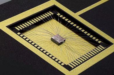
Professional Embedded Cavity PCB/Substrate Manufacturer, we mainly produce ultra-small bump pitch Cavity substrate/PCBs, ultra-small trace and spacing packaging cavity substrate and HDI Cavity PCBs.
Embedded Cavity PCBs or Substrates stand out as a specialized category of circuit boards or substrates utilized in electronic devices. What sets them apart is their deliberate design featuring an internal cavity or void, strategically incorporated to house and safeguard specific components—think integrated circuits (ICs) and other sensitive electronic elements.
Throughout the manufacturing process, particular attention is given to crafting this embedded cavity, contributing to a more streamlined and spatially efficient design. This deliberate design choice is a prevalent strategy aimed at boosting the performance and reliability of electronic devices. The embedded cavity provides a secure and shielded space for critical components, and depending on the application’s demands, the cavity may be filled with a protective material or intentionally left vacant.
These embedded cavity PCBs find their niche in scenarios where spatial limitations are a primary concern, and protecting sensitive components from external factors like heat, moisture, or electromagnetic interference is paramount. This design methodology finds widespread adoption across diverse industries, spanning telecommunications, aerospace, automotive, and consumer electronics.
What functions does Embedded Cavity PCB/Substrate serve?
Embedded Cavity PCBs or Substrates take on a myriad of roles, serving as essential components in electronic devices:
Guardians of Precision: Their primary responsibility lies in meticulously protecting specific components like integrated circuits (ICs) and intricate electronic elements. The embedded cavity serves as a protective barrier, strengthening these components against external factors like heat, moisture, and electromagnetic interference..
Pillars of Dependability: These PCBs serve as indispensable pillars in ensuring the overall dependability of electronic devices. By providing a secure sanctuary for critical components, they significantly contribute to sustained performance and longevity across various applications.
Architects of Efficiency: With a deliberate design featuring an embedded cavity, these PCBs excel in spatial efficiency. This design strategy proves invaluable in scenarios where spatial constraints necessitate a more compact and streamlined electronic device.
Magicians of Performance: The embedded cavity’s isolation capabilities work like magic, minimizing interference and noise to enhance signal integrity and overall performance in electronic devices.
Crafters of Customization: Offering a realm of design flexibility, these PCBs empower engineers to craft bespoke layouts tailored to the unique demands of each application. This extends to the freedom to choose specific protective materials for the embedded cavity.
Versatile Collaborators: Finding their niche across diverse industries, from telecommunications and aerospace to automotive and consumer electronics, these PCBs establish themselves as adaptable collaborators. Their versatility proves crucial in electronic devices where safeguarding components and optimizing space are paramount concerns.
In essence, Embedded Cavity PCBs emerge as meticulous guardians, reliable pillars, efficiency architects, performance magicians, customization crafters, and versatile collaborators, shaping the landscape of electronic devices.
What are the different types of Embedded Cavity PCB/Substrate?
Embedded Cavity PCBs or Substrates boast a rich diversity of types, each meticulously crafted to address distinct design intricacies and application exigencies:
Singular Sophistication – Single-Layer Embedded Cavity PCBs: Engineered with a lone substrate layer housing an embedded cavity, these PCBs shine in applications where simplicity and space efficiency take precedence.
Layered Dynamics – Multilayer Embedded Cavity PCBs: Through the strategic layering of multiple substrates with embedded cavities, this PCB variant introduces a level of complexity that provides flexibility for diverse routing and component connections.
Metallic Mastery – Metal Core Embedded Cavity PCBs: Featuring a core constructed from materials like aluminum or copper, these PCBs excel in efficient heat dissipation, making them a top choice for applications where thermal management is paramount.
Flexibility Unleashed – Flex PCBs with Embedded Cavities: Offering a harmonious blend of flexibility and space-saving advantages, these PCBs cater to applications requiring bending or flexibility.
Precision in High Frequencies – High-Frequency Embedded Cavity PCBs: Precision-engineered for high-frequency operations, these PCBs minimize signal loss and electromagnetic interference, with the embedded cavity playing a pivotal role in achieving superior performance.
RF (Radio Frequency) Virtuosity – RF Embedded Cavity PCBs: Tailored for optimal performance in radio frequency applications, these PCBs minimize signal loss, ensuring seamless transmission and reception of RF signals.
Hybrid Ingenuity – Hybrid Embedded Cavity PCBs: Through the fusion of diverse materials and technologies, these PCBs offer a bespoke solution tailored to meet the nuanced demands of various applications.
The selection of an Embedded Cavity PCB type hinges on factors such as application complexity, spatial constraints, thermal considerations, and frequency specifications. Manufacturers deftly craft designs to seamlessly align with the unique requirements of electronic devices integrating these PCBs.
How is Embedded Cavity PCB/Substrate related to IC packaging?
The symbiotic relationship between Embedded Cavity PCBs or Substrates and IC (Integrated Circuit) packaging revolves around their shared goal of providing a secure and streamlined environment for integrated circuits within electronic devices. Their interconnection can be delineated through the following facets:
Custodians of Circuitry: Both Embedded Cavity PCBs and IC packaging function as custodians for integrated circuits, offering protective measures against external elements. The embedded cavity in PCBs is strategically designed to house components like ICs, shielding them from environmental factors. Simultaneously, IC packaging involves encapsulation techniques to safeguard the integrated circuit from various stresses.
Spatial Optimization Strategies: The synergy between Embedded Cavity PCBs and IC packaging is evident in their commitment to optimizing spatial efficiency within electronic devices. Embedded Cavity PCBs achieve this through thoughtful void integration, while IC packaging, especially in advanced forms like chip-on-board (COB) or system-in-package (SiP), minimizes the physical footprint of the integrated circuit on the PCB.
Heat Dissipation Collaboration: Both technologies contribute to efficient thermal management. Embedded Cavity PCBs leverage material selection and the incorporation of a metal core to dissipate heat effectively. Simultaneously, IC packaging employs thermal management solutions such as heat sinks and thermal vias to address heat generated by the integrated circuit.
Customized Configurations: Embedded Cavity PCBs and IC packaging offer avenues for tailored customization to meet specific application requirements. The design flexibility of Embedded Cavity PCBs allows for the incorporation of specific cavities for diverse ICs and components. Similarly, IC packaging provides a variety of forms that can be customized based on the type of IC, application demands, and desired performance outcomes.
Preservation of Signal Integrity: Both Embedded Cavity PCBs and IC packaging play integral roles in preserving signal integrity. Embedded Cavity PCBs achieve this by minimizing electromagnetic interference through cavity design, while IC packaging considers signal routing, power distribution, and noise reduction to ensure optimal signal performance.
In essence, Embedded Cavity PCBs and IC packaging collaborate seamlessly to establish a protective, space-efficient, and tailored ecosystem for integrated circuits within electronic devices. This partnership contributes holistically to the reliability, performance, and thermal dynamics of the overall electronic system.
How does Embedded Cavity PCB/Substrate differ from traditional PCBs?
Embedded Cavity PCBs or Substrates diverge from traditional PCBs (Printed Circuit Boards) in significant ways, primarily stemming from the intentional integration of embedded voids or cavities. Here’s a nuanced exploration of their disparities:
Structural Deliberation:
Embedded Cavity PCBs: Exhibit a purposeful design, featuring internal voids strategically positioned within the substrate. These cavities are meticulously planned to provide a protective enclave for specific components.
Traditional PCBs: Embrace a uniform and solid structure, devoid of intentional internal voids. Components find their place on the PCB surface.
Component Lodging:
Embedded Cavity PCBs: Offer the flexibility of placing components within the embedded cavities, fostering a more compact and spatially efficient design.
Traditional PCBs: Witness components being mounted on the surface, confined to a two-dimensional plane.
Spatial Ingenuity:
Embedded Cavity PCBs: Geared towards space optimization by incorporating internal cavities, proving particularly advantageous in applications with spatial limitations.
Traditional PCBs: Leverage space based on the surface area of the PCB without the integration of internal voids.
Component Safeguarding:
Embedded Cavity PCBs: Extend a protective haven for specific components, shielding them from external elements like moisture, heat, and electromagnetic interference.
Traditional PCBs: Feature exposed components on the surface, lacking the additional protective layer provided by embedded cavities.
Thermal Dynamics:
Embedded Cavity PCBs: Designed with materials and structures to enhance heat dissipation, contributing to advanced thermal management strategies.
Traditional PCBs: Typically address heat dissipation through external means, such as heat sinks or fans.
Application Focus:
Embedded Cavity PCBs: Find prominence in applications where safeguarding components and optimizing space are paramount, such as in aerospace, automotive, and telecommunications.
Traditional PCBs: Widespread in various applications, particularly favored where space optimization and specific component protection are not primary considerations.
Manufacturing Nuances:
Embedded Cavity PCBs: Might involve additional manufacturing steps to create the embedded voids, introducing complexity to the fabrication process.
Traditional PCBs: Follow standard manufacturing procedures without the need for internal voids, resulting in a comparatively straightforward fabrication process.
In essence, the pivotal distinction lies in the deliberate inclusion of embedded cavities in the design of Embedded Cavity PCBs, affording advantages like component protection, spatial optimization, and enhanced thermal management—qualities not inherent in traditional PCBs. The selection between the two hinges on the unique requirements of the electronic application at hand.
What is the structure and production technology of Embedded Cavity PCB/Substrate?
Embedded Cavity PCBs or Substrates boast a sophisticated structure crafted through a meticulous production process that incorporates nuanced design considerations. Here’s a detailed exploration of their unique structure and the advanced technology involved in their production:
Structure:
Thoughtful Material Selection:
The selection of the PCB’s foundation revolves around the specific needs of the application. Materials like FR-4, Rogers, or other high-frequency options are considered.
Optional Metal Core Integration:
For added thermal efficiency, certain Embedded Cavity PCBs may feature a metal core, often composed of aluminum or copper. This integration enhances the PCB’s ability to dissipate heat effectively.
Strategic Cavity Design:
The design process intricately weaves strategically positioned cavities or voids within the substrate. These voids serve a dual purpose—providing a secure haven for specific components and optimizing spatial resources.
Application of Dielectric Layers:
Dielectric layers are introduced for insulation between various conductive layers. The choice of dielectric material is made with precision, considering both electrical and thermal properties.
Integration of Conductive Layers:
Conductive layers, featuring copper traces and planes, are expertly arranged to interconnect different components and elements on the PCB. The layout is meticulously crafted to accommodate the embedded cavities seamlessly.
Elevated Surface Finish:
A refined surface finish is applied to the PCB to shield it against oxidation and enhance solderability. Popular choices include HASL, ENIG, or OSP.
Production Technology:
Precision in Design Phase:
The design process involves the creation of a layout with meticulous attention to detail regarding the placement of embedded cavities, conductive traces, and critical components. Advanced design software ensures utmost accuracy.
Tailored Material Approach:
Substrate material and, if applicable, a metal core are customized to meet the specific thermal and electrical demands dictated by the application.
Artful Crafting of Cavities:
Cavities are delicately crafted through precise milling or routing processes, methodically removing material to carve out the intended voids.
Layer Assembly Expertise:
Different layers, comprising conductive and dielectric layers, are assembled with finesse according to design specifications. Perfect alignment is maintained to ensure accuracy.
Mastery in Lamination:
The layered stack undergoes a lamination process, subjecting it to heat and pressure to create a solid structure with securely bonded layers.
Drilling and Plating Precision:
Holes for component mounting and vias are drilled, and these holes are plated with conductive material to forge vital electrical connections between layers.
Art of Copper Etching:
Excess copper is selectively etched away, leaving behind the desired conductive traces and intricate patterns.
Finely Tuned Surface Finish:
The PCB undergoes meticulous surface finishing processes to fortify it against oxidation and enhance solderability.
Rigorous Quality Assurance:
A series of stringent tests and quality control measures are implemented to ensure that the finished PCB aligns seamlessly with required specifications and complies with industry standards.
Precision in Component Integration:
Components are delicately assembled onto the PCB, with meticulous attention to placing them within the purpose-designed embedded cavities.
In essence, the production technology of Embedded Cavity PCBs seamlessly integrates traditional PCB manufacturing processes with specialized steps tailored for the creation and integration of embedded voids. The flawless execution of these steps guarantees the functionality, reliability, and efficient thermal performance of the final product.
Frequently Asked Questions (FAQs)
How do Embedded Cavity PCBs differ from traditional PCBs?
Embedded Cavity PCBs stand out from traditional counterparts due to the deliberate inclusion of internal voids. These cavities serve purposes such as component protection, spatial efficiency, and enhanced thermal management.
In which industries are Embedded Cavity PCBs commonly used?
Embedded Cavity PCBs find applications in industries where safeguarding specific components, maximizing spatial resources, and efficient thermal control are critical. Examples include aerospace, automotive, telecommunications, and electronics with stringent requirements.
What sets the manufacturing process of Embedded Cavity PCBs apart?
The manufacturing process involves additional steps, such as milling or routing for cavity creation, adding complexity compared to traditional PCB fabrication.
Which materials are typically used in the production of Embedded Cavity PCBs?
Common base materials include FR-4, Rogers, or other high-frequency options. Additionally, manufacturers may integrate a metal core (aluminum or copper) for improved thermal performance.
What advantages do Embedded Cavity PCBs offer?
Benefits include component protection, efficient space utilization, and enhanced thermal management. These features make Embedded Cavity PCBs suitable for applications demanding reliability and compact design.
Is customization available for Embedded Cavity PCBs based on specific applications?
Yes, manufacturers often offer customization options to tailor Embedded Cavity PCBs for unique applications. This can involve designing cavities to accommodate specific components or adjusting board specifications to meet customer requirements.
How do Embedded Cavity PCBs contribute to thermal management?
The design may incorporate a metal core and specific materials to enhance heat dissipation. Additionally, internal voids allow for efficient airflow, contributing to effective thermal management within electronic devices.
Conclusion
In conclusion, Embedded Cavity PCBs/Substrates emerge as a specialized and sophisticated category of printed circuit boards deliberately designed with internal voids or cavities within the substrate. This intentional approach sets them apart from conventional PCBs, offering a host of advantages, including heightened component protection, optimized spatial utilization, and superior thermal management. These attributes position Embedded Cavity PCBs as optimal solutions for industries like aerospace, automotive, and telecommunications, where reliability and compact design are paramount.
The manufacturing process involves intricate procedures, including precision cavity creation through milling or routing, meticulous material selection (such as FR-4 or high-frequency materials), and the optional integration of a metal core for enhanced thermal efficiency. While this process introduces complexity compared to traditional PCB fabrication, it ensures tailored solutions that meet the specific requirements of diverse applications.
Quality control assumes a central role in the manufacturing process, ensuring both functionality and compliance with industry standards. Manufacturers often extend customization options, allowing Embedded Cavity PCBs to be finely tuned for the unique demands of each application. Thoughtful application of surface finishes, including HASL, ENIG, or OSP, takes into account factors such as oxidation resistance and solderability.
In essence, Embedded Cavity PCBs play a pivotal role in propelling electronic design forward by effectively addressing challenges related to component protection, spatial optimization, and thermal considerations. As technology evolves, the adaptability and specialized features of Embedded Cavity PCBs continue to propel innovation in electronic devices across various industries.