
Glass Package Substrates Manufacturer
Glass Package Substrates Manufacturer, Advanced glass substrate production process, The glass packaging substrate has lower warpage degree and is more resistant to high temperature, we offer Glass Package Substrates from 2 layer to 20 layers. we can do the microtrace and spacing with 9um/9um. same as the ABF base materials.
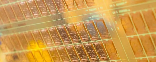
Glass Package Substrates (GPS) are a vital component in semiconductor packaging, revolutionizing the way electronic devices are constructed and functioning. Unlike conventional substrates made of silicon or ceramic, GPS utilizes glass as its base material. This choice offers several advantages, including superior thermal conductivity, enabling efficient heat dissipation, crucial for high-performance applications. Additionally, GPS allows for thinner substrates, contributing to the reduction of overall package size and weight, particularly beneficial in compact electronic devices like smartphones and wearables. Glass’s exceptional resistance to environmental factors such as moisture enhances the reliability and durability of the packaged semiconductor devices. GPS fabrication involves precision cutting, surface treatment, conductor and dielectric deposition, via formation, and surface finishing, ensuring high-quality substrates. These substrates find applications in various electronic components, including microprocessors, memory chips, sensors, and integrated circuits (ICs), supporting the advancement of technology in diverse industries. Overall, Glass Package Substrates play a pivotal role in enabling the performance, reliability, and miniaturization of electronic devices.
What is a Glass Package Substrate?
A Glass Package Substrate (GPS) is a type of packaging technology used in semiconductor manufacturing. It involves using glass as a substrate material instead of traditional materials like silicon or organic substrates.
In GPS technology, the semiconductor chips are mounted directly onto a glass substrate, which provides several advantages:
- Thermal Performance:Glass has excellent thermal conductivity, which helps in dissipating heat generated by the semiconductor devices more efficiently. This can improve the overall performance and reliability of the chips.
- Electrical Performance:Glass substrates can offer superior electrical insulation properties compared to other materials, reducing the risk of electrical interference and signal degradation.
- Miniaturization:Glass substrates can be made very thin, allowing for the creation of smaller and thinner packages. This is particularly important in applications where space is limited, such as in mobile devices.
- Reliability:Glass has excellent mechanical strength and dimensional stability, which can enhance the durability and reliability of the packaged semiconductor devices.
Overall, Glass Package Substrates are gaining popularity in semiconductor packaging due to their superior thermal, electrical, and mechanical properties, which contribute to improved performance, reliability, and miniaturization of electronic devices.
Advanced Glass Substrates
What are the Glass Package Substrate Design Guidelines?
Glass Package Substrate (GPS) design guidelines typically cover various aspects to ensure the reliability, performance, and manufacturability of the packaged semiconductor devices. Here are some common design guidelines:
- Thermal Management: Ensure efficient heat dissipation by optimizing the layout of components on the substrate to minimize thermal hotspots. Utilize the high thermal conductivity of glass to spread heat evenly across the substrate.
- Electrical Performance: Design the substrate layout to minimize signal interference, crosstalk, and impedance mismatches. Properly ground and shield sensitive components to maintain signal integrity.
- Mechanical Stability: Consider mechanical stress and strain during substrate manufacturing and assembly processes. Design features such as vias, routing, and component placement to minimize mechanical stress and ensure the reliability of the substrate.
- Material Selection: Choose glass materials with appropriate thermal, mechanical, and electrical properties for the specific application requirements. Consider factors such as coefficient of thermal expansion (CTE), dielectric constant, and glass transition temperature (Tg).
- Manufacturability: Design the substrate with manufacturability in mind, considering factors such as compatibility with fabrication processes, ease of assembly, and yield optimization. Ensure that the design meets industry standards and regulations.
- Package Size and Form Factor: Optimize the substrate size and form factor to meet the space constraints of the target application while maintaining adequate electrical and thermal performance.
- Reliability and Durability: Design the substrate to withstand environmental factors such as temperature variations, humidity, mechanical shock, and vibration. Perform thorough reliability testing to ensure long-term performance and durability of the packaged semiconductor device.
- Cost Optimization: Balance performance requirements with cost considerations by optimizing the substrate design for material usage, manufacturing complexity, and assembly processes.
- Signal and Power Integrity: Implement techniques such as controlled impedance routing, power distribution network design, and decoupling capacitor placement to ensure robust signal and power integrity.
- Interface Compatibility: Ensure compatibility with other components in the semiconductor packaging ecosystem, such as semiconductor dies, wire bonds, solder joints, and external interfaces.
These guidelines may vary depending on the specific requirements and constraints of the application, as well as the manufacturing processes and technologies involved. Working closely with semiconductor packaging experts and adhering to industry standards can help ensure the successful design and implementation of Glass Package Substrates.
What is the Glass Package Substrate Fabrication Process?
The fabrication process for Glass Package Substrates (GPS) involves several steps to create a substrate suitable for mounting and interconnecting semiconductor devices. Here is a generalized overview of the fabrication process:
- Glass Selection: Choose the appropriate type of glass material based on the specific requirements of the application, considering factors such as thermal conductivity, coefficient of thermal expansion (CTE), dielectric constant, and mechanical strength.
- Substrate Preparation: Begin by preparing the glass substrate by cutting it to the desired size and shape. This may involve processes such as cutting, grinding, and polishing to achieve the required surface finish and dimensional accuracy.
- Cleaning and Surface Treatment: Clean the glass substrate thoroughly to remove any contaminants or impurities that could affect subsequent processing steps. Apply surface treatments or coatings as needed to enhance adhesion and promote solderability.
- Etching and Patterning: Use photolithography or other patterning techniques to define the layout of circuit traces, vias, and other features on the glass substrate. Apply etching processes, such as wet chemical etching or dry plasma etching, to selectively remove glass material and create the desired patterns.
- Conductor Deposition: Deposit conductive materials, such as metals like copper or aluminum, onto the substrate surface to create circuit traces and interconnects. This can be achieved through techniques such as physical vapor deposition (PVD), chemical vapor deposition (CVD), or electroplating.
- Dielectric Layer Deposition: Deposit dielectric materials, such as silicon dioxide (SiO2) or polyimide, to insulate the conductive traces and provide electrical isolation between different layers of the substrate. This helps prevent short circuits and signal interference.
- Via Formation: Create vias or interconnect holes in the substrate to enable vertical connections between different layers of the substrate. This typically involves drilling or laser ablation followed by metallization to provide electrical continuity between adjacent layers.
- Surface Finish: Apply a surface finish to the substrate to protect the exposed conductive traces and facilitate soldering or wire bonding during the semiconductor device assembly process. Common surface finishes include immersion tin, immersion silver, and gold plating.
- Quality Control and Testing: Perform thorough inspection and testing of the fabricated substrate to ensure it meets the required specifications for dimensional accuracy, electrical performance, and reliability. This may include visual inspection, electrical continuity testing, and reliability testing under various environmental conditions.
- Packaging and Assembly: Once the glass substrate is fabricated and tested, it can be assembled with semiconductor devices, such as integrated circuits (ICs) or microelectromechanical systems (MEMS), using techniques such as flip-chip bonding, wire bonding, or soldering. The assembled package may undergo further testing and inspection before being integrated into electronic systems.
Throughout the fabrication process, strict quality control measures are typically employed to ensure the integrity and reliability of the Glass Package Substrate for use in various electronic applications.
How do you manufacture a Glass Package Substrate?
The fabrication process for Glass Package Substrates (GPS) involves several steps to create a substrate suitable for mounting and interconnecting semiconductor devices. Here is a generalized overview of the fabrication process:
- Glass Selection: Choose the appropriate type of glass material based on the specific requirements of the application, considering factors such as thermal conductivity, coefficient of thermal expansion (CTE), dielectric constant, and mechanical strength.
- Substrate Preparation: Begin by preparing the glass substrate by cutting it to the desired size and shape. This may involve processes such as cutting, grinding, and polishing to achieve the required surface finish and dimensional accuracy.
- Cleaning and Surface Treatment: Clean the glass substrate thoroughly to remove any contaminants or impurities that could affect subsequent processing steps. Apply surface treatments or coatings as needed to enhance adhesion and promote solderability.
- Etching and Patterning: Use photolithography or other patterning techniques to define the layout of circuit traces, vias, and other features on the glass substrate. Apply etching processes, such as wet chemical etching or dry plasma etching, to selectively remove glass material and create the desired patterns.
- Conductor Deposition: Deposit conductive materials, such as metals like copper or aluminum, onto the substrate surface to create circuit traces and interconnects. This can be achieved through techniques such as physical vapor deposition (PVD), chemical vapor deposition (CVD), or electroplating.
- Dielectric Layer Deposition: Deposit dielectric materials, such as silicon dioxide (SiO2) or polyimide, to insulate the conductive traces and provide electrical isolation between different layers of the substrate. This helps prevent short circuits and signal interference.
- Via Formation: Create vias or interconnect holes in the substrate to enable vertical connections between different layers of the substrate. This typically involves drilling or laser ablation followed by metallization to provide electrical continuity between adjacent layers.
- Surface Finish: Apply a surface finish to the substrate to protect the exposed conductive traces and facilitate soldering or wire bonding during the semiconductor device assembly process. Common surface finishes include immersion tin, immersion silver, and gold plating.
- Quality Control and Testing: Perform thorough inspection and testing of the fabricated substrate to ensure it meets the required specifications for dimensional accuracy, electrical performance, and reliability. This may include visual inspection, electrical continuity testing, and reliability testing under various environmental conditions.
- Packaging and Assembly: Once the glass substrate is fabricated and tested, it can be assembled with semiconductor devices, such as integrated circuits (ICs) or microelectromechanical systems (MEMS), using techniques such as flip-chip bonding, wire bonding, or soldering. The assembled package may undergo further testing and inspection before being integrated into electronic systems.
Throughout the fabrication process, strict quality control measures are typically employed to ensure the integrity and reliability of the Glass Package Substrate for use in various electronic applications.
How much should a Glass Package Substrate cost?
The cost of a Glass Package Substrate (GPS) can vary widely depending on several factors including the complexity of the design, the size of the substrate, the materials used, manufacturing processes involved, and the volume of production. Here are some factors that can influence the cost:
- Design Complexity: The complexity of the substrate design, including the number of layers, the density of circuitry, and the precision of features, can significantly impact the cost. More complex designs typically require more sophisticated manufacturing processes, which can increase costs.
- Materials Used: The cost of materials, particularly the type of glass and any additional coatings or surface treatments, will affect the overall cost of the GPS. High-performance glass materials with specific properties may be more expensive than standard glass substrates.
- Manufacturing Processes: The manufacturing processes involved in fabricating the GPS, such as photolithography, etching, deposition, and assembly, contribute to the overall cost. Advanced manufacturing techniques and equipment may incur higher costs.
- Volume of Production: Economies of scale play a significant role in determining the cost of GPS. Higher production volumes generally lead to lower per-unit costs due to spreading fixed costs over a larger number of units. Conversely, low-volume production runs may result in higher unit costs.
- Quality and Reliability Requirements: Meeting stringent quality and reliability standards may involve additional testing and quality control measures, which can increase costs. High-reliability applications may require more rigorous testing and inspection procedures.
- Supplier and Location: The choice of supplier and manufacturing location can also impact the cost of GPS. Labor costs, overhead expenses, and supply chain logistics can vary depending on the location of the manufacturing facility.
- Customization and Special Features: Customized features or special requirements, such as specific surface finishes, unique substrate shapes, or additional functionalities, can add to the overall cost of the GPS.
Due to the diverse range of factors influencing the cost, it’s challenging to provide a specific price without knowing the specific requirements of the GPS in question. Typically, GPS manufacturers provide quotes based on the customer’s specifications and volume requirements. It’s advisable to work closely with GPS suppliers to obtain accurate cost estimates based on the desired specifications and production volumes.
What is Glass Package Substrate base material?
The base material for Glass Package Substrates (GPS) is, unsurprisingly, glass. However, not just any glass will do; manufacturers typically use specialized types of glass with specific properties tailored to meet the requirements of semiconductor packaging.
Two common types of glass used as base materials for GPS are:
- Borosilicate Glass: Borosilicate glass is a type of glass with a low coefficient of thermal expansion (CTE), which means it expands and contracts less with changes in temperature compared to other types of glass. This property makes borosilicate glass well-suited for applications where thermal stability is important, such as semiconductor packaging.
- Alumino-Silicate Glass: Alumino-silicate glass is another type of glass commonly used in GPS manufacturing. It offers excellent mechanical strength, thermal shock resistance, and chemical durability. These properties make alumino-silicate glass suitable for demanding applications where reliability and durability are critical.
Glass substrates used in GPS manufacturing are typically engineered to have specific thermal, mechanical, and electrical properties to meet the requirements of semiconductor packaging. These properties include thermal conductivity, dielectric constant, dimensional stability, and compatibility with various fabrication and assembly processes.
Overall, the choice of glass material as the base substrate for GPS is crucial in ensuring the reliability, performance, and manufacturability of the packaged semiconductor devices.
Which company makes Glass Package Substrates?
There are many companies worldwide engaged in the production of Glass Package Substrates (GPS). Some of the well-known companies include Corning from the United States, Schott from Germany, Nippon Electric Glass (NEG) from Japan, Samsung Corning Precision Materials (SCP) from South Korea, and North Glass from China, among others. These companies have extensive experience and technological expertise in the GPS field, offering various types and specifications of GPS products to meet different application requirements.
Our company is a leading enterprise specializing in semiconductor packaging technology. With advanced GPS production lines and a professional technical team, we are committed to providing high-quality and highly reliable GPS products. As experts in GPS manufacturing, our company can offer the following advantages:
- Technical Strength: We have an experienced and specialized R&D team with profound knowledge of semiconductor packaging technology and processes. We continuously innovate and invest in research and development to meet the ever-changing needs of customers.
- Advanced Equipment: Equipped with advanced GPS production equipment and process technologies, including lithography equipment, thin film deposition equipment, etching equipment, and more. The application of these equipment and technologies enables us to achieve efficient and precise GPS production.
- Quality Management: We strictly adhere to the ISO quality management system and implement rigorous quality control measures to ensure stable and reliable product quality. We conduct comprehensive quality inspection and testing to ensure that each batch of products meets customer requirements and standards.
- Customization: We can provide customized GPS products according to customer requirements, including different sizes, thicknesses, materials, and process requirements. We work closely with customers to ensure satisfactory solutions.
- Quick Response: We prioritize communication and cooperation with customers, promptly responding to their needs and providing timely technical support and services. Customer satisfaction is at the core of our business, and we continuously improve service quality and customer experience.
In summary, our company has extensive experience and professional technical expertise in the GPS field, providing competitive advantages. We are committed to offering high-quality, high-performance GPS products, delivering reliable solutions for our customers’ applications.
What are the 7 qualities of good customer service?
Good customer service is essential for building strong relationships with customers and fostering loyalty. Here are seven qualities that characterize good customer service:
- Responsiveness:Good customer service involves being prompt and responsive to customer inquiries, requests, and concerns. Customers appreciate timely assistance and solutions to their problems, whether it’s answering questions, resolving issues, or providing assistance with product or service-related matters.
- Empathy: Empathy is the ability to understand and share the feelings of others, including customers. Good customer service representatives demonstrate empathy by actively listening to customers, acknowledging their concerns, and showing genuine concern for their needs and emotions. This helps build trust and rapport with customers.
- Professionalism: Good customer service is delivered with professionalism and courtesy. Customer service representatives should conduct themselves professionally at all times, maintaining a positive attitude, using appropriate language and tone, and adhering to company policies and standards.
- Knowledgeability: Customers expect customer service representatives to be knowledgeable about the products or services offered by the company. Good customer service involves having a thorough understanding of the company’s offerings, policies, procedures, and industry standards. This enables representatives to provide accurate information and effective assistance to customers.
- Problem-Solving Skills: Good customer service requires strong problem-solving skills to address customer issues and resolve conflicts effectively. Customer service representatives should be resourceful, creative, and proactive in finding solutions to customer problems, even in challenging situations. This helps turn negative experiences into positive outcomes and enhances customer satisfaction.
- Consistency: Consistency is key to delivering good customer service. Customers expect consistent experiences each time they interact with a company, whether it’s through phone calls, emails, live chat, or in-person interactions. Consistent service delivery builds trust and reliability, leading to increased customer satisfaction and loyalty.
- Personalization: Good customer service often involves personalizing interactions to meet the unique needs and preferences of individual customers. This can include addressing customers by name, remembering their past interactions and preferences, and tailoring solutions to their specific situations. Personalized service makes customers feel valued and appreciated, strengthening their connection to the company.
By embodying these qualities, businesses can deliver exceptional customer service experiences that drive customer satisfaction, loyalty, and long-term success.
FAQs
What is a Glass Package Substrate (GPS)?
A GPS is a type of substrate used in semiconductor packaging, where glass serves as the base material instead of traditional materials like silicon or ceramic.
What are the advantages of using Glass Package Substrates?
GPS offers several advantages, including excellent thermal conductivity for efficient heat dissipation, smaller and lighter packages due to thinner substrates, high resistance to moisture and environmental factors, and enhanced reliability and durability.
What are Glass Package Substrates used for?
GPS is used in various semiconductor packaging applications, including microprocessors, memory chips, sensors, and integrated circuits (ICs), particularly in high-performance and high-reliability applications.
How are Glass Package Substrates fabricated?
The fabrication process for GPS involves several steps, including glass cutting, cleaning, surface treatment, patterning, conductor and dielectric layer deposition, via formation, surface finish, quality control, and assembly with semiconductor devices.
What types of glass are used in Glass Package Substrates?
Common types of glass used in GPS include borosilicate glass and alumino-silicate glass, chosen for their thermal, mechanical, and electrical properties suitable for semiconductor packaging.
What factors influence the cost of Glass Package Substrates?
The cost of GPS can vary depending on factors such as design complexity, materials used, manufacturing processes, volume of production, quality and reliability requirements, customization, and supplier and location.
Which companies manufacture Glass Package Substrates?
Several companies worldwide are involved in the production of GPS, including Corning, Schott, Nippon Electric Glass (NEG), Samsung Corning Precision Materials (SCP), and North Glass, among others.