
Microtrace PCB manufacturing
Microtrace PCB manufacturing, 9UM trace and 9um gap, we use the ABF to produce the Microtrace PCB or BGA substrates. when your trace are more bigger than 25um. we can use the BT materials or other types materials. we offer the Microtrace PCB and Microtrace BGA substrates from 2 layer to 22 layers.
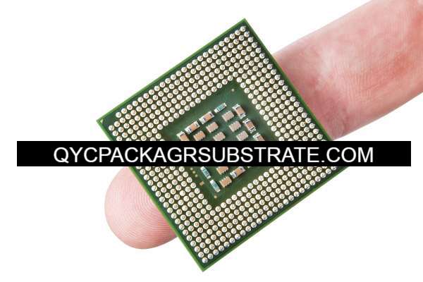
Microtrace PCBs represent a pinnacle of modern circuit board technology, featuring ultra-fine conductive pathways etched onto the surface with precision. These microscopic traces enable high-density circuitry, allowing for the integration of more components into smaller spaces. With their advanced manufacturing techniques, such as laser ablation or photolithography, Microtrace PCBs achieve unparalleled levels of accuracy and reliability in signal routing. They offer numerous benefits, including enhanced signal integrity, reduced electromagnetic interference, and improved miniaturization capabilities. Microtrace PCBs find applications across various industries, from consumer electronics like smartphones and wearables to critical systems in medical devices, aerospace, and telecommunications. Their ability to deliver exceptional performance in compact form factors makes them indispensable for modern electronic devices where space is limited and performance is paramount. In essence, Microtrace PCBs embody innovation and precision, driving the advancement of electronic technology into ever smaller and more powerful devices.
What is a Microtrace PCB?
A Microtrace PCB, or Microscopic Trace Printed Circuit Board, is an advanced technology in circuit board design and manufacturing. It incorporates microscopic traces, which are ultra-fine conductive pathways etched onto the surface of the PCB. These traces allow for the precise routing of electrical signals within electronic devices.
The microscopic traces in a Microtrace PCB are much thinner and more closely spaced than those found in traditional PCBs. This enables higher circuit density, meaning more components can be packed into a smaller space, making it ideal for compact electronic devices like smartphones, tablets, and wearables.
The manufacturing process of Microtrace PCBs typically involves advanced techniques such as laser ablation or photolithography to achieve the precise dimensions and spacing required for the microscopic traces. This level of precision is crucial for ensuring signal integrity and minimizing signal interference in high-frequency applications.
Microtrace PCBs offer several advantages over conventional PCBs, including improved signal integrity, reduced electromagnetic interference (EMI), and enhanced miniaturization capabilities. These benefits make them well-suited for applications where space is limited, and high-performance is essential, such as in consumer electronics, medical devices, aerospace systems, and telecommunications equipment.
Overall, Microtrace PCBs represent a cutting-edge solution for achieving higher performance and functionality in electronic devices while maintaining a compact form factor.
What are Microtrace PCB Design Guidelines?
Microtrace PCB design guidelines are established to ensure that best practices are followed in the design and manufacturing of Microtrace PCBs to achieve optimal performance and reliability. Here are some common Microtrace PCB design guidelines:
- Microtrace Layout:Designers should minimize the length of signal paths and use straight lines and 45-degree corners whenever possible to reduce signal delay and loss. Layouts should consider the flow of signals to minimize signal interference and crosstalk.
- Trace Width and Spacing:Microtrace PCBs typically have very small trace widths and spacings, often in the range of a few micrometers or smaller. Designers must ensure that trace widths and spacings are within the manufacturer’s capabilities and account for possible manufacturing tolerances.
- Ground and Power Planes:In Microtrace PCBs, the layout of ground and power planes is crucial for providing good signal integrity and EMI suppression. Designers should minimize the area of ground loops and ensure adequate connections between ground planes and signal layers.
- Layer Stacking and Spacing:Microtrace PCBs often utilize multilayer designs to accommodate more traces and components. Designers should pay attention to the order of stacking and layer spacing to ensure good coupling between signal and power planes and minimize crosstalk.
- High-Frequency Characteristics:For high-frequency applications such as RF and microwave circuits, special attention is required in Microtrace PCB design. Trace and component layouts should be optimized to minimize the length and loss of signal transmission paths and avoid signal loops.
- EMI Management:Designers should take measures to minimize electromagnetic interference in Microtrace PCBs. This includes using ground and power planes for shielding and arranging traces and components reasonably to reduce electromagnetic radiation.
- Manufacturability:When designing Microtrace PCBs, manufacturability and cost-effectiveness must be considered. Designers should choose manufacturing processes compatible with microtrace requirements and take into account manufacturing tolerances and limitations.
In summary, Microtrace PCB design guidelines cover many aspects including layout, trace width and spacing, layer stacking, high-frequency characteristics, EMI management, and manufacturability. Following these guidelines ensures the design of high-performance, reliable Microtrace PCBs.
Microtrace PCB
What is the Microtrace PCB Fabrication Process?
The fabrication process of Microtrace PCBs involves several steps to create the ultra-fine conductive pathways and achieve the precise dimensions required for microscopic traces. Here’s an overview of the typical fabrication process:
- Substrate Preparation:The process begins with preparing the substrate material, usually a laminate composed of layers of fiberglass reinforced with epoxy resin. The substrate is cleaned and treated to ensure proper adhesion of the conductive layers.
- Layer Alignment:For multilayer PCBs, multiple substrate layers are aligned and stacked together. Alignment is crucial to ensure that the conductive layers match up correctly during subsequent processing steps.
- Copper Deposition:A thin layer of copper is deposited onto the substrate surface using techniques such as electroplating or chemical vapor deposition (CVD). This copper layer serves as the conductive material for the traces.
- Photoresist Application:A layer of photoresist, a light-sensitive material, is applied over the copper surface. This photoresist will be patterned to define the locations of the traces.
- Exposure and Development:A photomask containing the desired trace patterns is placed over the photoresist-coated substrate, and ultraviolet light is used to expose the photoresist. The exposed areas of the photoresist become soluble, while the unexposed areas remain insoluble. The substrate is then developed to remove the unexposed photoresist, revealing the copper beneath.
- Etching:The exposed copper is etched away using chemical etchants, leaving behind the desired trace patterns on the substrate. The etching process must be highly precise to achieve the ultra-fine dimensions required for Microtrace PCBs.
- Strip and Clean:After etching, the remaining photoresist is stripped away, leaving only the copper traces on the substrate. The PCB is thoroughly cleaned to remove any residues from the fabrication process.
- Surface Finish:Surface finish options such as gold plating or immersion silver may be applied to the copper traces to improve solderability and protect against oxidation.
- Quality Control:The fabricated PCB undergoes rigorous quality control inspections to ensure that the trace dimensions, spacing, and alignment meet the specified requirements. Any defects or irregularities are identified and corrected.
- Final Inspection:Once the fabrication process is complete, the finished Microtrace PCB undergoes a final inspection to verify its functionality and integrity before being released for use in electronic devices.
Overall, the fabrication process of Microtrace PCBs requires advanced techniques and precision to achieve the ultra-fine dimensions and high-density circuitry essential for compact electronic devices.
How do you manufacture a Microtrace PCB?
Manufacturing a Microtrace PCB involves a series of intricate processes designed to create extremely fine conductive pathways on the circuit board. Here’s a step-by-step guide to manufacturing a Microtrace PCB:
- Design Preparation:The process starts with the design of the PCB using specialized software. Designers create the layout, including the placement of components and the routing of traces, paying close attention to signal integrity and minimizing interference.
- Substrate Selection:Choose a substrate material suitable for Microtrace PCBs, often a high-quality laminate composed of layers of fiberglass reinforced with epoxy resin. The substrate material should have excellent dimensional stability and electrical properties.
- Cleaning and Preparation:Clean the substrate material thoroughly to remove any contaminants or residues that could affect the adhesion of subsequent layers. Treat the substrate surface to promote adhesion and ensure uniformity.
- Copper Deposition:Deposit a thin layer of copper onto the substrate surface through processes like electroplating or chemical vapor deposition (CVD). This copper layer will serve as the conductive material for the traces.
- Photoresist Application:Apply a layer of photoresist, a light-sensitive material, over the copper-coated substrate. The photoresist will be patterned to define the locations of the traces.
- Exposure and Development:Use a photomask containing the desired trace patterns and expose the photoresist-coated substrate to ultraviolet (UV) light. The exposed areas of the photoresist become soluble, while the unexposed areas remain insoluble. Develop the substrate to remove the unexposed photoresist, revealing the underlying copper.
- Etching:Etch away the exposed copper using chemical etchants, leaving behind the desired trace patterns on the substrate. The etching process must be precise to achieve the ultra-fine dimensions required for Microtrace PCBs.
- Strip and Clean:Remove the remaining photoresist from the substrate, leaving only the copper traces. Thoroughly clean the PCB to remove any residues from the fabrication process.
- Surface Finish:Apply a surface finish to the copper traces to improve solderability and protect against oxidation. Common surface finishes include gold plating, immersion silver, or tin/lead solder.
- Quality Control:Perform rigorous quality control inspections to ensure that the trace dimensions, spacing, and alignment meet the specified requirements. Use automated optical inspection (AOI) and other testing methods to detect any defects or irregularities.
- Final Inspection:Once manufacturing is complete, conduct a final inspection to verify the functionality and integrity of the Microtrace PCB before it is released for use in electronic devices.
Manufacturing a Microtrace PCB requires advanced techniques, precision equipment, and attention to detail to achieve the ultra-fine dimensions and high-density circuitry essential for compact electronic devices.
How much should a Microtrace PCB cost?
The cost of a Microtrace PCB can vary widely depending on several factors, including the complexity of the design, the number of layers, the size of the board, the materials used, and the quantity ordered. However, Microtrace PCBs tend to be more expensive than traditional PCBs due to the advanced manufacturing processes and the precision required to create ultra-fine conductive pathways.
As a rough estimate, the cost of a Microtrace PCB can range from a few dollars for simple designs with a small quantity to several hundred dollars or more for complex designs with multiple layers and high quantities. Factors that can affect the cost include:
- Design Complexity:PCBs with intricate trace patterns or high-density components may require more advanced manufacturing processes, driving up the cost.
- Number of Layers:Multi-layer Microtrace PCBs typically cost more to manufacture than single-layer PCBs due to the additional fabrication steps and materials required.
- Materials:The choice of substrate material, copper thickness, and surface finish can all impact the cost of the PCB.
- Quantity:Ordering larger quantities of Microtrace PCBs often results in lower per-unit costs due to economies of scale.
- Lead Time:Expedited manufacturing or delivery options may come with additional fees.
To get an accurate cost estimate for a specific Microtrace PCB project, it’s best to consult with PCB manufacturers or suppliers. They can provide quotes based on your design specifications and production requirements. Additionally, some online PCB fabrication services offer instant quotes based on uploaded design files and selected specifications.
What is Microtrace PCB base material?
The base material used for Microtrace PCBs is typically a laminate composed of layers of fiberglass reinforced with epoxy resin. This type of laminate is commonly referred to as FR-4 (Flame Retardant 4) and is widely used in the electronics industry for its excellent electrical insulation properties, mechanical strength, and dimensional stability.
FR-4 laminates consist of a woven fiberglass cloth impregnated with an epoxy resin binder. This material combination provides the PCB with high strength and rigidity while also offering good thermal and chemical resistance. The fiberglass reinforcement helps to prevent the PCB from warping or deforming during the manufacturing process and while in use.
In addition to FR-4, other materials such as polyimide (PI) or liquid crystal polymer (LCP) may also be used for Microtrace PCBs, especially in applications that require higher temperature resistance or flexibility. These materials offer similar electrical properties to FR-4 but with different mechanical and thermal characteristics.
The choice of base material for a Microtrace PCB depends on factors such as the intended application, operating environment, and specific requirements of the design. Designers often select a base material that provides the best balance of electrical performance, mechanical strength, thermal stability, and cost for their particular application.
Which company makes Microtrace PCB?
Currently, many well-known PCB manufacturers are capable of producing Microtrace PCBs. Some of the major manufacturers include AT&S, Zuken, Mitsubishi Electric, Samsung Electro-Mechanics, and others. These companies possess advanced manufacturing equipment and technologies to meet various design requirements for Microtrace PCBs, including ultra-fine conductive pathways, high-density layouts, and precise manufacturing processes.
As for our company, we also have the capability to produce Microtrace PCBs and possess extensive experience and expertise in this field. We have advanced manufacturing equipment and a skilled technical team capable of providing high-quality Microtrace PCB solutions to our customers.
Our manufacturing process employs state-of-the-art technologies and strict quality control standards to ensure that each Microtrace PCB exhibits excellent performance and reliability. Our engineering team is capable of providing customized designs according to customer requirements and offering professional technical support and advice to ensure that customer needs and expectations are met.
Furthermore, we are committed to continuous improvement and innovation to keep pace with the evolving trends in Microtrace PCB technology and provide our customers with more advanced solutions. We always prioritize customer satisfaction and strive to be a trusted partner by offering the best products and services to our customers.
In summary, our company has the capability to produce Microtrace PCBs and is willing to collaborate with customers to develop and manufacture high-performance circuit board products that meet their needs.
What are the 7 qualities of good customer service?
Good customer service is characterized by several key qualities that help build positive relationships with customers and ensure their satisfaction. Here are seven qualities of good customer service:
- Responsive:Good customer service is prompt and responsive to customers’ needs and inquiries. Responding quickly to questions, concerns, and requests demonstrates that the company values its customers’ time and is committed to addressing their needs promptly.
- Empathetic:Empathy is crucial in customer service. It involves understanding and acknowledging customers’ emotions, concerns, and perspectives. Showing empathy helps customers feel understood and valued, leading to better rapport and trust.
- Effective Communication:Clear and effective communication is essential for providing good customer service. Customer service representatives should communicate clearly, listen actively to customers’ concerns, and provide helpful and relevant information or solutions.
- Knowledgeable: Good customer service requires having a thorough understanding of the company’s products, services, policies, and procedures. Knowledgeable representatives can provide accurate information, answer questions, and offer appropriate solutions to customer issues.
- Proactive: Proactive customer service involves anticipating customers’ needs and addressing potential issues before they arise. Proactive measures, such as providing proactive updates or offering additional assistance, demonstrate attentiveness and dedication to customer satisfaction.
- Professionalism:Professionalism is essential in all customer interactions. Customer service representatives should maintain a professional demeanor, remain courteous and respectful, and handle challenging situations calmly and diplomatically.
- Empowerment:Empowering customer service representatives to make decisions and take action to resolve customer issues fosters a sense of ownership and accountability. Empowered representatives can provide timely and effective solutions, leading to greater customer satisfaction and loyalty.
By embodying these qualities, businesses can deliver exceptional customer service experiences that leave a positive impression and foster long-term relationships with customers.
FAQs
What is a Microtrace PCB?
A Microtrace PCB, or Microscopic Trace Printed Circuit Board, is an advanced technology in circuit board design and manufacturing. It incorporates ultra-fine conductive pathways, allowing for high-density circuitry and precise signal routing within electronic devices.
What are the benefits of Microtrace PCBs?
Microtrace PCBs offer several advantages, including higher circuit density, improved signal integrity, reduced electromagnetic interference (EMI), and enhanced miniaturization capabilities. They are well-suited for compact electronic devices where space is limited and high performance is crucial.
How are Microtrace PCBs manufactured?
The manufacturing process of Microtrace PCBs involves several steps, including substrate preparation, copper deposition, photoresist application, exposure and development, etching, surface finish, and quality control inspections. Advanced techniques such as laser ablation or photolithography are often used to achieve precise dimensions and spacing for the microscopic traces.
What applications are Microtrace PCBs used in?
Microtrace PCBs are used in a wide range of applications, including consumer electronics (such as smartphones, tablets, and wearables), medical devices, aerospace systems, telecommunications equipment, and high-frequency RF/microwave circuits.
What design considerations are important for Microtrace PCBs?
Designers must consider factors such as trace layout, width, and spacing, ground and power plane configuration, high-frequency characteristics, EMI management, and manufacturability when designing Microtrace PCBs. These considerations are crucial for ensuring optimal performance and reliability.
What is the cost of Microtrace PCBs?
The cost of Microtrace PCBs can vary depending on factors such as design complexity, number of layers, substrate material, surface finish, quantity ordered, and lead time. It’s best to consult with PCB manufacturers for a cost estimate based on specific project requirements.