
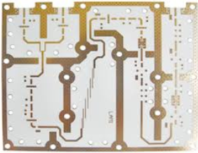
Multilayer ceramic PCB manufacturing
Multilayer ceramic PCB Manufacturing, rofessional ceramic production line, professional production team. we offer Ceramic PCBs and BGA Ceramic package substrates from 1 layer to 20 layers. Multilayer Ceramic PCBs are advanced electronic circuit boards that utilize ceramic material as the substrate instead of traditional fiberglass epoxy. These PCBs consist of multiple layers of ceramic material, with conductive traces and components embedded within. Known for their exceptional thermal conductivity, Multilayer Ceramic PCBs efficiently dissipate heat, making them ideal for high-power and high-frequency applications. Their excellent electrical insulation properties ensure reliable performance even in harsh environments with temperature variations and moisture exposure. Multilayer Ceramic PCBs offer compact designs and high component density, making them suitable for space-constrained applications such as aerospace, automotive, telecommunications, and medical devices. With superior reliability, stability, and signal integrity, Multilayer Ceramic PCBs are preferred for critical electronic systems where performance and durability are paramount.
What is a Multilayer Ceramic PCB?
Multilayer ceramic PCB manufacturing.High speed and high frequency material packaging substrate manufacturing. Advanced packaging substrate production process and technology
A Multilayer Ceramic PCB (Printed Circuit Board) is a type of electronic circuit board that uses ceramic material as the substrate instead of the more commonly used fiberglass epoxy. It incorporates multiple layers of ceramic material, each containing conductive traces, vias, and other components necessary for electronic circuits.
Here are some key features and characteristics of Multilayer Ceramic PCBs:
- Ceramic Material: Unlike traditional PCBs, which use fiberglass epoxy as the substrate, Multilayer Ceramic PCBs utilize ceramic material. Ceramic offers several advantages such as high thermal conductivity, excellent electrical insulation properties, and stability over a wide range of temperatures.
- Multiple Layers: Multilayer Ceramic PCBs consist of multiple layers of ceramic material stacked together. These layers are interconnected using conductive traces and vias, allowing for complex and compact circuit designs.
- High Density: Due to the ability to create multiple layers, Multilayer Ceramic PCBs can achieve high circuit density. This allows for the integration of more components and functionality into a smaller footprint, making them ideal for applications where space is limited.
- High Frequency Applications: Multilayer Ceramic PCBs are well-suited for high-frequency applications due to the low dielectric constant of ceramic material. This characteristic enables better signal integrity and reduced signal loss at high frequencies.
- Thermal Management: Ceramic material has excellent thermal conductivity, which helps dissipate heat more effectively compared to traditional PCB substrates like FR-4. This makes Multilayer Ceramic PCBs suitable for applications requiring efficient thermal management.
- Reliability: Multilayer Ceramic PCBs offer high reliability and stability, particularly in harsh environments where temperature fluctuations or moisture can affect the performance of electronic components.
- Cost: Multilayer Ceramic PCBs are generally more expensive compared to traditional PCBs due to the cost of ceramic material and the specialized manufacturing processes involved. However, for certain applications where performance and reliability are paramount, the benefits may outweigh the higher cost.
Overall, Multilayer Ceramic PCBs are preferred for high-performance applications that demand reliability, compactness, and efficient thermal management, such as aerospace, automotive, telecommunications, and high-frequency electronic devices.
Multilayer ceramic PCB
What are the Multilayer Ceramic PCB Design Guidelines?
Designing Multilayer Ceramic PCBs requires careful consideration of various factors to ensure optimal performance and reliability. Here are some design guidelines:
- Layer Stackup: Plan the layer stackup carefully, considering the signal integrity, power distribution, and thermal management requirements. Typically, high-speed signal layers are placed closer to the center of the stackup to minimize signal distortion.
- Dielectric Material Selection: Choose the appropriate ceramic material with the desired dielectric constant and thermal conductivity for the specific application requirements.
- Signal Routing: Follow best practices for signal routing, such as maintaining controlled impedance traces, minimizing signal reflections, and avoiding sharp bends or right angles in traces.
- Power and Ground Planes: Ensure proper power and ground distribution by incorporating dedicated power and ground planes. These planes should be placed close to each other to minimize loop inductance and provide a low-impedance return path.
- Decoupling Capacitors: Place decoupling capacitors strategically throughout the board to provide local energy storage and reduce power supply noise.
- Thermal Management: Integrate thermal vias and thermal pads to dissipate heat efficiently from critical components. Ensure proper airflow and heat sinking if required.
- Component Placement: Place components strategically to minimize signal interference and optimize signal integrity. Keep high-speed components closer to each other and avoid placing sensitive components near noisy sources.
- Via Design: Optimize via placement and design to minimize signal discontinuities and impedance mismatches. Use blind or buried vias for high-density designs where appropriate.
- Design for Manufacturing (DFM): Consider manufacturing constraints early in the design process to avoid issues during fabrication. Ensure that the design complies with the capabilities of the chosen manufacturing process.
- Reliability Considerations: Design the PCB to withstand environmental factors such as temperature variations, moisture, and mechanical stress. Follow industry standards and guidelines for reliability testing and qualification.
- EMI/EMC Compliance: Design the PCB to meet electromagnetic interference (EMI) and electromagnetic compatibility (EMC) requirements by implementing proper shielding, filtering, and grounding techniques.
- Documentation: Maintain comprehensive documentation of the design, including schematics, layout files, and design notes, to facilitate future modifications and troubleshooting.
By adhering to these Multilayer Ceramic PCB design guidelines, designers can ensure that their PCBs meet performance, reliability, and manufacturability requirements for a wide range of applications.
What is the Multilayer Ceramic PCB Fabrication Process?
The fabrication process for Multilayer Ceramic PCBs involves several steps to create the multiple layers of ceramic material with embedded conductive traces and components. Here’s an overview of the typical fabrication process:
- Design Preparation: The process begins with the design of the PCB using computer-aided design (CAD) software. Designers specify the layer stackup, component placement, routing, and other details according to the project requirements.
- Material Selection: Ceramic material with suitable properties such as dielectric constant, thermal conductivity, and mechanical strength is selected based on the application requirements. The ceramic material often comes in the form of sheets or tapes.
- Layer Preparation: The selected ceramic material is prepared for the fabrication process. This may involve cutting the material into appropriate sizes and shapes for the PCB layers.
- Conductive Traces Printing: Conductive traces are printed onto the ceramic layers using techniques such as screen printing, inkjet printing, or photolithography. These traces form the interconnections between components and layers.
- Component Placement: Electronic components such as resistors, capacitors, and integrated circuits are placed onto the ceramic layers using pick-and-place machines or manual assembly methods. The components are positioned according to the PCB design.
- Lamination: The ceramic layers with embedded traces and components are stacked together to form the multilayer structure. The layers are bonded together using pressure and heat, often in a process known as lamination. This step ensures proper alignment and adhesion between the layers.
- Via Formation: Vias, which are small holes that allow electrical connections between different layers, are drilled or formed in the laminated stack. Techniques such as laser drilling or mechanical drilling may be used depending on the via size and density requirements.
- Conductive Via Filling: The vias are filled with conductive material, typically a metal paste or ink, to establish electrical connections between the layers.
- Firing: The assembled PCB stack undergoes a firing process in a kiln or furnace at high temperatures. This step sinters the ceramic material and activates the conductive traces, forming a solid and durable structure.
- Surface Finishing: Surface finishing processes such as metallization, solder mask application, and surface coating are performed to improve solderability, protect the PCB, and provide additional functionality if required.
- Quality Control and Testing: The fabricated Multilayer Ceramic PCB undergoes thorough inspection and testing to ensure that it meets the specified requirements for electrical performance, dimensional accuracy, and reliability.
- Final Assembly: Once the PCB passes quality control, it may undergo final assembly, where additional components or connectors are attached before being integrated into the final product.
By following these steps, manufacturers can produce Multilayer Ceramic PCBs with precise dimensions, excellent electrical properties, and high reliability for various electronic applications.
How do you manufacture a Multilayer Ceramic PCB?
Manufacturing a Multilayer Ceramic PCB involves several steps to create the multiple layers of ceramic material with embedded conductive traces and components. Here’s a detailed overview of the typical manufacturing process:
- Design Preparation: The process starts with the design of the Multilayer Ceramic PCB using computer-aided design (CAD) software. Designers specify the layer stackup, component placement, routing, and other details according to the project requirements.
- Material Preparation: Ceramic material with suitable properties such as dielectric constant, thermal conductivity, and mechanical strength is selected based on the application requirements. The ceramic material is often in the form of sheets or tapes. These materials are cut or shaped into individual layers according to the PCB design.
- Conductive Traces Printing: Conductive traces are printed onto the ceramic layers using techniques such as screen printing, inkjet printing, or photolithography. These traces form the interconnections between components and layers. Special conductive inks or pastes are used for this purpose.
- Component Placement: Electronic components such as resistors, capacitors, and integrated circuits are placed onto the ceramic layers using pick-and-place machines or manual assembly methods. The components are positioned according to the PCB design.
- Layer Stacking: The ceramic layers with embedded traces and components are stacked together to form the multilayer structure. The layers are aligned carefully to ensure proper registration and electrical continuity. Adhesive materials may be used to temporarily hold the layers together during subsequent processing steps.
- Lamination: The assembled PCB stack undergoes a lamination process to bond the layers together permanently. This is typically done under heat and pressure to ensure proper adhesion and consolidation of the ceramic layers.
- Via Formation: Vias, which are small holes that allow electrical connections between different layers, are formed in the laminated stack. Techniques such as laser drilling or mechanical drilling may be used depending on the via size and density requirements.
- Conductive Via Filling: The vias are filled with conductive material, usually a metal paste or ink, to establish electrical connections between the layers. This step may involve screen printing or dispensing the conductive material into the vias.
- Firing: The assembled PCB stack undergoes a firing process in a kiln or furnace at high temperatures. This step sinters the ceramic material and activates the conductive traces, forming a solid and durable structure. The firing process may take several hours or even days depending on the thickness of the ceramic layers and the firing temperature.
- Surface Finishing: Surface finishing processes such as metallization, solder mask application, and surface coating are performed to improve solderability, protect the PCB, and provide additional functionality if required.
- Quality Control and Testing: The fabricated Multilayer Ceramic PCB undergoes thorough inspection and testing to ensure that it meets the specified requirements for electrical performance, dimensional accuracy, and reliability.
- Final Assembly: Once the PCB passes quality control, it may undergo final assembly, where additional components or connectors are attached before being integrated into the final product.
By following these steps, manufacturers can produce Multilayer Ceramic PCBs with precise dimensions, excellent electrical properties, and high reliability for various electronic applications.
How much should a Multilayer Ceramic PCB cost?
The cost of a Multilayer Ceramic PCB can vary significantly depending on several factors, including:
- Size and Complexity: Larger and more complex PCBs with higher layer counts, finer traces, and smaller features will generally cost more to manufacture.
- Material: The type and quality of ceramic material used in the PCB can affect the cost. High-performance ceramic materials with specific properties may be more expensive than standard ceramics.
- Manufacturing Process: The chosen manufacturing process, such as screen printing, photolithography, or laser drilling, can impact the cost. Processes requiring specialized equipment or multiple fabrication steps may incur higher expenses.
- Component Density: PCBs with a high component density, requiring intricate routing and placement, may be more expensive due to the increased complexity of assembly.
- Volume: The quantity of PCBs ordered can affect the unit cost. Larger production runs typically result in lower per-unit costs due to economies of scale.
- Lead Time: Expedited manufacturing or shorter lead times may incur additional costs compared to standard turnaround times.
- Additional Services: Additional services such as surface finishing, testing, and assembly can add to the overall cost of the PCB.
It’s challenging to provide an exact cost without specific details about the PCB’s design requirements, quantity, and manufacturing specifications. However, Multilayer Ceramic PCBs generally tend to be more expensive than traditional FR-4 PCBs due to the specialized materials and manufacturing processes involved.
For a rough estimate, Multilayer Ceramic PCBs may range from a few dollars to several hundred dollars per square inch, with higher costs for more complex designs or specialized requirements. It’s advisable to consult with PCB manufacturers and obtain quotes based on your specific project needs to determine the precise cost.
What is Multilayer Ceramic PCB base material?
The base material used for Multilayer Ceramic PCBs is ceramic. Unlike traditional PCBs, which often use fiberglass epoxy or other organic materials as the substrate, Multilayer Ceramic PCBs utilize ceramic material for their substrate.
Ceramic materials offer several advantages for PCB applications, including:
- High Thermal Conductivity: Ceramic materials have high thermal conductivity, allowing for efficient dissipation of heat generated by electronic components. This property is particularly beneficial for high-power applications or those requiring effective thermal management.
- Excellent Electrical Insulation: Ceramics provide excellent electrical insulation properties, helping to prevent electrical leakage and short circuits between conductive traces. This characteristic is crucial for maintaining signal integrity and preventing electrical failures.
- Stability Across Temperature Range: Ceramics exhibit stability across a wide temperature range, making them suitable for use in environments with extreme temperature variations. They maintain their structural integrity and electrical properties even under harsh conditions.
- Low Dielectric Constant: The low dielectric constant of ceramic materials minimizes signal loss and distortion, making Multilayer Ceramic PCBs suitable for high-frequency applications requiring precise signal transmission.
- Mechanical Strength: Ceramics are inherently strong and rigid, providing mechanical stability to the PCB. This strength helps prevent warping or flexing of the PCB during handling or operation.
- Chemical Resistance: Ceramic materials are resistant to many chemicals, moisture, and environmental contaminants, enhancing the durability and reliability of Multilayer Ceramic PCBs in challenging operating environments.
Common types of ceramic materials used for Multilayer Ceramic PCBs include alumina (aluminum oxide), aluminum nitride, and silicon carbide. These materials offer different properties and characteristics suited to various applications and performance requirements.
Overall, the choice of ceramic material for Multilayer Ceramic PCBs contributes to their high performance, reliability, and suitability for demanding electronic applications.
Which company makes Multilayer Ceramic PCB?
Several companies have extensive experience and technology in manufacturing Multilayer Ceramic PCBs. Some well-known companies include Hitachi Chemical, Murata Manufacturing, and Samsung Electro-Mechanics. These companies possess leading technology and production capabilities in the field of Multilayer Ceramic PCBs, providing high-quality products for various industries.
In our company, we also have the capability to produce Multilayer Ceramic PCBs. As a professional electronics manufacturing enterprise, we adhere to rigorous processes and utilize advanced production equipment to meet customer demands for high-performance, high-reliability PCBs.
We have an experienced engineering team that can provide comprehensive support from design to production. We can customize the design of Multilayer Ceramic PCBs according to customer requirements and employ advanced manufacturing processes to ensure product quality and performance. Our production processes strictly adhere to international standards and industry norms to ensure that our products meet customer requirements and expectations.
Additionally, we prioritize quality control and after-sales service. We have a complete quality management system in place to rigorously control each process and ensure the stability and reliability of product quality. At the same time, we offer timely after-sales support to help customers resolve any issues encountered during use.
Overall, our company has the capability to produce Multilayer Ceramic PCBs and provide customized solutions according to customer needs. We are committed to meeting customer requirements with high-quality products and excellent service, providing reliable support for the success of our customers’ projects.
What are the 7 qualities of good customer service?
Good customer service is characterized by several key qualities that contribute to positive experiences and satisfaction for customers. Here are seven qualities of good customer service:
- Responsiveness: Good customer service involves promptly addressing customer inquiries, concerns, and requests. Responding to customers in a timely manner demonstrates respect for their time and shows that their needs are valued.
- Empathy: Empathy is essential in understanding and acknowledging customers’ emotions, concerns, and perspectives. Showing empathy allows customer service representatives to connect with customers on a personal level and provide more effective assistance.
- Clear Communication: Effective communication is crucial in customer service interactions. Customer service representatives should communicate clearly and concisely, using language that is easy for customers to understand. Providing accurate information and setting realistic expectations helps to avoid misunderstandings and build trust.
- Problem-solving Skills: Good customer service involves being proactive in identifying and resolving customer issues and challenges. Customer service representatives should possess strong problem-solving skills, including the ability to analyze situations, brainstorm solutions, and take appropriate action to address customer concerns.
- Professionalism:Professionalism encompasses a range of qualities, including politeness, respectfulness, and reliability. Customer service representatives should maintain a professional demeanor at all times, treating customers with courtesy and demonstrating competence in handling their needs.
- Consistency: Consistency is key in delivering good customer service experiences. Customers expect consistent levels of service across all interactions and touchpoints with a company. Consistency helps to build trust and loyalty by demonstrating reliability and dependability.
- Follow-up and Follow-through: Good customer service extends beyond the initial interaction. Following up with customers to ensure their needs have been met and following through on commitments demonstrates commitment to customer satisfaction. Following up also provides an opportunity to gather feedback and address any remaining concerns.
By embodying these qualities, businesses can deliver exceptional customer service experiences that foster customer loyalty, retention, and positive word-of-mouth referrals.
FAQs
What is a Multilayer Ceramic PCB?
A Multilayer Ceramic PCB is an electronic circuit board that utilizes ceramic material as the substrate instead of traditional fiberglass epoxy. It consists of multiple layers of ceramic material with embedded conductive traces and components, offering high performance and reliability.
What are the advantages of Multilayer Ceramic PCBs?
Multilayer Ceramic PCBs offer several advantages, including high thermal conductivity, excellent electrical insulation, stability across temperature variations, low dielectric constant for high-frequency applications, and resistance to environmental factors such as moisture and chemicals.
What are the typical applications of Multilayer Ceramic PCBs?
Multilayer Ceramic PCBs are commonly used in high-performance electronic devices and systems, including aerospace, automotive, telecommunications, medical devices, and industrial equipment. They are particularly suitable for applications requiring compact size, high reliability, and efficient thermal management.
How are Multilayer Ceramic PCBs manufactured?
The manufacturing process for Multilayer Ceramic PCBs involves steps such as layer stackup planning, conductive traces printing, component placement, lamination, via formation, firing, surface finishing, quality control, and testing. The process utilizes specialized equipment and techniques to create the multiple layers of ceramic material with embedded components.
What factors affect the cost of Multilayer Ceramic PCBs?
The cost of Multilayer Ceramic PCBs depends on factors such as size and complexity, material selection, manufacturing process, component density, volume, lead time, additional services, and quality requirements. Generally, Multilayer Ceramic PCBs tend to be more expensive than traditional PCBs due to the specialized materials and manufacturing processes involved.
Where can I find suppliers of Multilayer Ceramic PCBs?
Suppliers of Multilayer Ceramic PCBs can be found through online directories, trade shows, industry associations, and referrals from colleagues or business partners. It’s essential to research suppliers carefully, considering factors such as their experience, capabilities, quality standards, and customer reviews.
What considerations should I keep in mind when designing Multilayer Ceramic PCBs?
When designing Multilayer Ceramic PCBs, consider factors such as layer stackup, material selection, signal routing, power and ground planes, thermal management, component placement, via design, design for manufacturing (DFM), reliability considerations, and electromagnetic interference (EMI) compliance.