
RF/microwave PCB Manufacturer
RF/microwave PCB Manufacturer. High speed and high frequency material microwave PCBs and BGA packaging substrate Manufacturer. Advanced packaging substrate production process and technology.
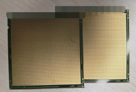
RF/microwave PCBs are specialized printed circuit boards designed to efficiently transmit and receive high-frequency signals, typically in the radio frequency (RF) and microwave frequency ranges. These PCBs are engineered with materials and structures optimized for the unique challenges posed by high-frequency applications. They often utilize substrates with low dielectric constants, such as PTFE-based laminates (e.g., Teflon), to minimize signal loss and distortion. Controlled impedance traces and transmission line routing techniques are employed to maintain signal integrity and minimize reflections. RF/microwave PCBs are essential components in various industries, including telecommunications, radar systems, satellite communication, and wireless networking. Their reliability, performance, and ability to handle high-frequency signals make them critical for enabling efficient and robust communication systems and electronic devices in today’s interconnected world.
What is an RF/microwave PCB?
An RF/microwave PCB (Printed Circuit Board) is a specialized type of PCB designed to work with radio frequency (RF) and microwave signals. These boards are engineered to provide reliable transmission and reception of high-frequency signals without significant loss or distortion.
RF/microwave PCBs differ from standard PCBs in several ways:
- Material:They are often made using materials optimized for RF performance, such as PTFE (Polytetrafluoroethylene) or FR-4 with high copper content.
- Construction:RF/microwave PCBs may have different layer configurations, with specific layer thicknesses and arrangements optimized for signal integrity and controlled impedance.
- Features:They may include specialized features like grounded coplanar waveguides, microstrip or stripline transmission lines, and controlled impedance traces to maintain signal integrity.
- Component Placement:Components are placed and routed with care to minimize signal distortion, electromagnetic interference (EMI), and signal loss.
- Shielding:RF/microwave PCBs often incorporate shielding techniques to minimize interference from external sources and prevent signal leakage.
These PCBs are commonly used in applications such as telecommunications, radar systems, satellite communication, wireless networking, and RF/microwave circuits in electronic devices.
What are the RF/microwave PCB Design Guidelines?
Designing RF/microwave PCBs requires careful consideration of various factors to ensure optimal performance. Here are some general guidelines:
- Choose the Right Substrate Material:Select a substrate material with appropriate dielectric properties and low loss tangent to minimize signal loss. Common materials include PTFE (e.g., Teflon) and high-frequency laminates like Rogers or Arlon.
- Controlled Impedance: Maintain controlled impedance for transmission lines to minimize signal reflections and ensure signal integrity. Use trace width, spacing, and substrate thickness to achieve the desired impedance.
- Grounding:Ensure a solid ground plane for proper signal return paths and to minimize electromagnetic interference (EMI). Use stitching vias to connect ground planes on different layers.
- Component Placement:Place components strategically to minimize signal distortion and interference. Group RF components together and keep them away from high-speed digital components to reduce crosstalk.
- Transmission Line Routing:Route transmission lines carefully to minimize signal loss and distortion. Use straight traces, avoid sharp bends, and maintain consistent impedance along the trace length.
- Balanced Routing:Keep signal traces and ground traces balanced to minimize electromagnetic radiation and improve signal integrity.
- Shielding:Use shielding techniques like grounded coplanar waveguides, shielded enclosures, or RF shielding cans to reduce EMI and prevent signal leakage.
- Via Placement:Place vias strategically to minimize signal distortion and maintain controlled impedance. Use via fences or stitching vias to connect ground planes and reduce electromagnetic interference.
- Avoidance of Resonances:Design PCB layouts to avoid resonances at critical frequencies, which can cause signal degradation or unwanted radiation.
- Simulation and Testing:Use electromagnetic simulation tools to analyze and optimize the PCB layout for RF performance. Additionally, perform thorough testing and validation to ensure compliance with design specifications.
Following these guidelines can help ensure the successful design and performance of RF/microwave PCBs in various applications.
RF/microwave PCB
What is the RF/microwave PCB Fabrication Process?
The fabrication process for RF/microwave PCBs involves several steps to create a board optimized for high-frequency performance. Here’s a general overview of the process:
- Design:The process begins with the design of the PCB layout using specialized RF/microwave design software. Engineers create the layout based on the circuit schematic, considering factors like controlled impedance, signal integrity, and component placement.
- Material Selection:Choose a substrate material with suitable dielectric properties for RF/microwave applications. Common materials include PTFE-based laminates (e.g., Teflon), high-frequency FR-4, or specialty materials like Rogers or Arlon laminates.
- Preparation of Substrate Material:The chosen substrate material is prepared by cutting it to the required size and cleaning it thoroughly to remove any contaminants that could affect the PCB’s performance.
- Copper Cladding:Apply a thin layer of copper foil to both sides of the substrate material. This copper cladding forms the conductive layers of the PCB.
- Etching:Use photolithography or another etching method to selectively remove copper from the clad substrate, leaving behind the desired circuit traces and pads. Etching is typically performed using chemical processes or plasma etching.
- Drilling:Drill holes (vias) in the substrate material at locations where electrical connections between layers or components are needed. These vias will be plated to provide conductivity between layers.
- Plating: Plate the vias and any exposed copper surfaces to ensure electrical conductivity and improve the reliability of the PCB. Plating can be done using electroplating or other methods to deposit a thin layer of metal (usually copper) on the exposed surfaces.
- Solder Mask Application:Apply a solder mask over the PCB surface to protect the copper traces from oxidation and facilitate soldering of components. The solder mask is applied in areas where components will be soldered, leaving the copper traces exposed.
- Silkscreen Printing:Optionally, apply a silkscreen layer to add component labels, reference designators, and other identifying information to the PCB surface.
- Surface Finish:Apply a surface finish to protect the exposed copper surfaces and facilitate soldering. Common surface finishes for RF/microwave PCBs include immersion gold, ENIG (Electroless Nickel Immersion Gold), or immersion silver.
- Final Inspection:Inspect the finished PCB for any defects or imperfections that could affect its performance. Check for proper alignment of traces, presence of shorts or opens, and overall quality of the fabrication.
- Testing:Perform electrical testing to verify the functionality and performance of the fabricated PCB. This may include tests for impedance matching, signal integrity, and reliability under operating conditions.
By following these steps, manufacturers can produce RF/microwave PCBs with the necessary characteristics for reliable high-frequency operation.
How do you manufacture an RF/microwave PCB?
Manufacturing RF/microwave PCBs involves a series of steps that require specialized equipment and techniques to ensure high-frequency performance. Here’s an overview of the manufacturing process:
- Design Preparation:Engineers create the PCB layout using specialized RF/microwave design software, considering factors such as controlled impedance, signal integrity, and component placement.
- Material Selection:Choose a substrate material with appropriate dielectric properties for RF/microwave applications. Common materials include PTFE-based laminates (e.g., Teflon), high-frequency FR-4, or specialty materials like Rogers or Arlon laminates.
- Panelization:Arrange multiple PCB designs on a larger panel to optimize manufacturing efficiency. Panelization allows for simultaneous processing of multiple PCBs during fabrication.
- Material Cutting:Cut the substrate material to the required size using precision cutting equipment. This step ensures that each PCB panel is properly sized and aligned for subsequent processing.
- Copper Cladding:Apply a thin layer of copper foil to both sides of the substrate material. This copper cladding serves as the conductive layers of the PCB and provides the basis for creating circuit traces.
- Lamination:Stack multiple layers of substrate material and copper foil together to form a multilayered PCB structure. The layers are laminated together under heat and pressure using a hydraulic press or vacuum lamination equipment.
- Drilling:Precision-drill holes (vias) in the PCB panel at locations where electrical connections between layers or components are needed. High-precision CNC drilling machines are used to ensure accuracy and consistency.
- Electroless Copper Deposition:Coat the drilled vias and exposed copper surfaces with a thin layer of electroless copper to provide electrical conductivity and facilitate plating.
- Electroplating:Plate the PCB panel with additional copper to increase the thickness of the conductive layers and provide mechanical strength. Electroplating is performed using an electrolytic bath containing copper ions.
- Etching:Use photolithography or another etching method to selectively remove excess copper from the PCB panel, leaving behind the desired circuit traces and pads. Etching is typically performed using chemical processes or plasma etching.
- Solder Mask Application:Apply a solder mask over the PCB surface to protect the copper traces from oxidation and facilitate soldering of components. The solder mask is applied in areas where components will be soldered, leaving the copper traces exposed.
- Silkscreen Printing:Optionally, apply a silkscreen layer to add component labels, reference designators, and other identifying information to the PCB surface.
- Surface Finish: Apply a surface finish to protect the exposed copper surfaces and facilitate soldering. Common surface finishes for RF/microwave PCBs include immersion gold, ENIG (Electroless Nickel Immersion Gold), or immersion silver.
- Routing and Profiling:Use CNC routing equipment to cut the individual PCBs from the panel and remove excess material. This step separates the finished PCBs from the larger panel.
- Final Inspection:Inspect the finished PCBs for any defects or imperfections that could affect their performance. Check for proper alignment of traces, presence of shorts or opens, and overall quality of the fabrication.
- Testing:Perform electrical testing to verify the functionality and performance of the manufactured PCBs. This may include tests for impedance matching, signal integrity, and reliability under operating conditions.
By following these steps, manufacturers can produce RF/microwave PCBs with the necessary characteristics for reliable high-frequency operation. Each step requires precision and attention to detail to ensure the quality and performance of the final product.
How much should an RF/microwave PCB cost?
The cost of an RF/microwave PCB can vary significantly depending on several factors:
- Complexity of Design:PCBs with complex designs, multiple layers, tight tolerances, and high-density components will typically cost more to manufacture due to increased production time and material requirements.
- Material Selection:The choice of substrate material and copper thickness can significantly impact the cost. Specialty materials optimized for RF/microwave applications, such as high-frequency laminates like Rogers or Arlon, tend to be more expensive than standard FR-4.
- Manufacturing Process:Certain manufacturing processes, such as controlled impedance routing, fine-pitch component assembly, and high-precision drilling, may add to the overall cost of production.
- Quantities: Larger production quantities generally result in lower per-unit costs due to economies of scale. However, prototype or low-volume runs may incur higher costs per unit.
- Additional Features:Extra features such as impedance matching structures, RF shielding, gold plating, or specialized surface finishes can contribute to increased costs.
- Supplier and Location:Different PCB manufacturers may offer varying pricing structures based on their capabilities, expertise, overhead costs, and geographic location.
As a rough estimate, the cost of a standard RF/microwave PCB could range from tens to hundreds of dollars per unit for prototype or small-volume production runs, while larger quantities may yield costs in the single-digit dollar range or less per unit. It’s essential to obtain quotes from multiple PCB manufacturers and carefully consider the trade-offs between cost, quality, and lead times to determine the best option for your specific requirements.
What is RF/microwave PCB base material?
The base material used for RF/microwave PCBs plays a crucial role in determining the performance of the board at high frequencies. Some common materials used for RF/microwave PCBs include:
- PTFE (Polytetrafluoroethylene):PTFE-based materials, such as Teflon, are widely used for RF/microwave applications due to their low dielectric constant, low loss tangent, and stable electrical properties over a wide range of frequencies. PTFE materials offer excellent signal integrity and are suitable for high-frequency circuits.
- FR-4 with High Copper Content:FR-4 is a standard substrate material used in PCB manufacturing, but for RF/microwave applications, versions with higher copper content are often preferred. High-copper FR-4 laminates provide improved thermal conductivity and better RF performance compared to standard FR-4.
- Rogers Laminates: Rogers Corporation produces a range of high-performance laminates specifically designed for RF/microwave applications. These laminates are engineered to offer low dielectric loss, tight controlled impedance, and excellent dimensional stability, making them suitable for high-frequency designs.
- Arlon Laminates:Arlon is another manufacturer of high-performance laminates tailored for RF/microwave applications. Arlon laminates typically offer low loss, stable dielectric properties, and good thermal conductivity, making them suitable for demanding high-frequency circuits.
- Isola Laminates:Isola produces a variety of laminates suitable for RF/microwave applications, offering low loss, high thermal conductivity, and consistent electrical performance across a wide frequency range.
These materials come in different grades and specifications, allowing designers to choose the most suitable material for their specific application requirements, whether it’s for high-frequency communication systems, radar applications, satellite systems, or other RF/microwave circuits. Each material has its advantages and trade-offs in terms of cost, performance, and manufacturability, so careful consideration is essential when selecting the base material for an RF/microwave PCB.
Which company makes RF/microwave PCB?
Many companies worldwide specialize in producing high-frequency (RF) and microwave PCBs, possessing advanced technology and extensive experience to meet the unique demands of high-frequency signals. For example, Rogers Corporation, Arlon, and Isola are well-known suppliers of high-performance PCB materials in the industry. The materials they produce are often used in manufacturing RF/microwave PCBs.
In addition, some specialized PCB manufacturers, such as TTM Technologies, AT&S in Europe, and Nanya Technology in Asia, also offer dedicated RF/microwave PCB manufacturing services. These companies have advanced production equipment and sophisticated processes to produce PCBs that meet the requirements of high-frequency applications.
Our company also has the capability to manufacture RF/microwave PCBs. We use high-quality substrate materials such as PTFE (Polytetrafluoroethylene, commercially known as Teflon), Rogers, or Arlon’s high-frequency materials. These materials have low dielectric constants and low loss characteristics, making them ideal for high-frequency signal transmission. Our manufacturing process is meticulous and rigorous, including:
- Design and Simulation:Our design team uses advanced design software such as Altium Designer or Cadence for PCB design and electromagnetic simulation to ensure optimized designs that meet the special requirements of RF/microwave applications.
- Material Cutting and Preparation:Precision cutting equipment is used to process materials to ensure the accuracy of substrate dimensions and cleanliness.
- Multilayer Lamination Technology:High-precision hot pressing technology is used to laminate multilayer boards, ensuring tight bonding between layers and consistent electrical performance.
- Precision Drilling and Copper Plating:High-precision drilling equipment is used for micro-hole drilling, and electroless copper plating technology is used to ensure the conductivity and reliability of conductive holes.
- Circuit Etching:Advanced etching technology is used to precisely remove unwanted copper, forming fine lines and pads.
- Surface Treatment:PCB surfaces are protected and optimized through processes such as gold plating, electroless nickel immersion gold (ENIG), etc., to improve solderability and corrosion resistance.
- Assembly and Testing:After PCB manufacturing is completed, we provide assembly and comprehensive electrical performance testing services to ensure that each PCB meets the highest performance standards.
Through our professional processes, we can provide high-quality RF/microwave PCB products for a variety of high-frequency applications such as communications, radar, aerospace, etc. Our production capacity and strict quality control ensure that we can meet the high-performance standards required by customers in high-frequency applications.
What are the 7 qualities of good customer service?
Good customer service is essential for maintaining customer satisfaction and loyalty. Here are seven qualities that contribute to effective customer service:
- Empathy:Empathy involves understanding and sharing the feelings of customers. A good customer service representative empathizes with customers’ concerns and frustrations, demonstrating genuine care and concern for their needs.
- Active Listening:Active listening is the ability to fully concentrate, understand, respond, and remember what is being said by the customer. It involves giving full attention to the customer, asking clarifying questions, and paraphrasing to ensure accurate understanding.
- Patience:Patience is crucial in customer service, especially when dealing with difficult or irate customers. A good customer service representative remains calm and composed, even in challenging situations, and takes the time to address customer concerns thoroughly.
- Effective Communication:Effective communication involves conveying information clearly, concisely, and respectfully. Good customer service representatives communicate with customers in a friendly and professional manner, using language that is easy to understand and free of jargon.
- Problem-Solving Skills:Good customer service representatives possess strong problem-solving skills to resolve customer issues efficiently and effectively. They identify root causes of problems, explore possible solutions, and work collaboratively with customers to find satisfactory resolutions.
- Product Knowledge:A good understanding of the company’s products or services is essential for providing helpful assistance to customers. Customer service representatives should be knowledgeable about the features, benefits, and uses of the products/services they support, enabling them to answer questions accurately and provide useful recommendations.
- Consistency:Consistency in customer service involves delivering a consistently high level of service across all interactions and touchpoints. Customers appreciate reliability and predictability in their interactions with a company, so maintaining consistency in service quality, response times, and problem resolution builds trust and confidence.
By embodying these qualities, customer service teams can create positive experiences for customers, foster loyalty, and contribute to the overall success of the business.
FAQs
What is an RF/microwave PCB?
An RF/microwave PCB is a specialized type of printed circuit board designed to handle high-frequency signals typically found in radio frequency (RF) and microwave applications.
What makes RF/microwave PCBs different from standard PCBs?
RF/microwave PCBs are designed with materials and structures optimized for high-frequency performance. They often use specialized substrates with low dielectric constants and controlled impedance traces to minimize signal loss and distortion.
What are the typical applications of RF/microwave PCBs?
RF/microwave PCBs are used in a wide range of applications, including telecommunications, radar systems, satellite communication, wireless networking, and RF/microwave circuits in electronic devices.
What are the key design considerations for RF/microwave PCBs?
Key design considerations include controlled impedance, signal integrity, grounding techniques, component placement, transmission line routing, shielding, and avoidance of resonances.
What materials are commonly used in RF/microwave PCBs?
Common materials include PTFE-based laminates (e.g., Teflon), high-frequency FR-4 with high copper content, Rogers laminates, Arlon laminates, and Isola laminates.
What are some challenges in manufacturing RF/microwave PCBs?
Challenges include maintaining tight tolerances for controlled impedance, minimizing signal loss and distortion, ensuring proper grounding and shielding, and achieving consistency in high-frequency performance.
How can I ensure the reliability of RF/microwave PCBs?
Reliability can be ensured through thorough testing and validation, including electrical testing for impedance matching and signal integrity, environmental testing for temperature and humidity resistance, and reliability testing for long-term performance.
What are some common design mistakes to avoid in RF/microwave PCBs?
Common mistakes include inadequate grounding, improper transmission line routing, insufficient isolation between RF and digital components, and ignoring manufacturability constraints.
How do I choose the right PCB manufacturer for RF/microwave applications?
Look for manufacturers with expertise in high-frequency PCB design and fabrication, advanced manufacturing capabilities, a track record of quality and reliability, and the ability to provide custom solutions tailored to your specific requirements.
What are the cost considerations for RF/microwave PCBs?
Costs can vary depending on factors such as complexity of design, choice of materials, manufacturing processes, quantities, and additional features. It’s essential to balance cost considerations with the need for high-quality, high-performance PCBs.