
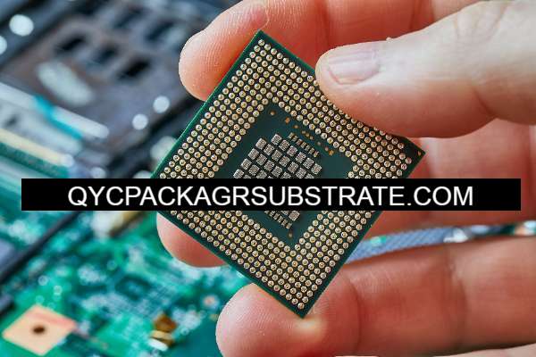
Substrate package Manufacturer
What is Substrate Package?
Substrate package Manufacturer. we can produce the best samllest bump pitch with 100um, the best smallest trace are 9um. and the smallest gap are 9um. most of the design are 15um to 30um trace and spacing.
A substrate package, often referred to simply as a substrate, is a type of packaging used in integrated circuits (ICs) and semiconductor devices. It serves as a base or foundation upon which semiconductor components are mounted and interconnected to form a functional electronic device.
Substrate packages are typically made of materials such as ceramics, silicon, or various types of organic substrates. They provide mechanical support for the semiconductor components, facilitate electrical connections between components, and may also offer thermal management capabilities.
In the context of PCB (Printed Circuit Board) design, substrate packages are commonly used for mounting integrated circuits (ICs), such as microprocessors, memory chips, and other types of semiconductor devices. These packages come in various forms, including leaded packages (such as dual in-line packages or DIPs), surface-mount packages (such as quad flat packages or QFPs), and ball grid arrays (BGAs).
Overall, the substrate package plays a crucial role in the performance, reliability, and manufacturability of semiconductor devices and electronic systems.
Substrate package Manufacturer
What are the Functions of Substrate Package?
The substrate package serves several important functions in the design and operation of integrated circuits (ICs) and semiconductor devices. Some of the key functions include:
Mechanical Support: The substrate package provides a solid foundation for mounting and securing semiconductor components. It helps protect the delicate semiconductor die from physical damage due to handling, assembly, and operation.
Electrical Connections: The substrate package facilitates electrical connections between the semiconductor die and external circuitry. It typically contains conductive traces, pads, or pins that connect the die to the rest of the circuit, enabling signal transmission, power supply, and other electrical functions.
Heat Dissipation: Many substrate packages incorporate thermal management features to dissipate heat generated by the semiconductor components during operation. This helps prevent overheating and ensures the reliable performance of the device over its operational lifetime.
Signal Integrity: The substrate package plays a role in maintaining signal integrity by minimizing parasitic effects such as signal loss, crosstalk, and impedance mismatch. Careful design of the substrate layout and interconnects helps ensure that signals propagate efficiently and accurately within the device.
Integration of Passive Components: Some substrate packages may include embedded passive components such as resistors, capacitors, and inductors. These components can be integrated directly into the substrate to save space, reduce assembly complexity, and improve overall system performance.
Environmental Protection: The substrate package provides a protective enclosure for the semiconductor die, shielding it from environmental factors such as moisture, dust, and contaminants. This helps enhance the reliability and longevity of the device, particularly in harsh operating conditions.
Overall, the substrate package plays a critical role in the performance, reliability, and functionality of integrated circuits and semiconductor devices, providing mechanical support, electrical connectivity, thermal management, signal integrity, and environmental protection.
What are the Different Types of Substrate Package?
There are several different types of substrate packages used in the semiconductor industry, each offering specific characteristics and advantages suited to different applications. Some of the common types of substrate packages include:
Ceramic Packages: Ceramic packages are made from materials such as alumina (Al2O3) or aluminum nitride (AlN). They offer excellent thermal conductivity, mechanical strength, and reliability, making them suitable for high-performance applications that require robust packaging. Ceramic packages come in various forms, including dual in-line packages (DIPs), ceramic quad flat packages (CQFPs), and ceramic ball grid arrays (CBGAs).
Plastic Packages: Plastic packages, also known as plastic encapsulated packages (PEPs), are made from thermosetting or thermoplastic materials. They are cost-effective, lightweight, and easy to manufacture in high volumes, making them popular for consumer electronics and other mass-produced devices. Plastic packages come in different configurations such as plastic dual in-line packages (PDIPs), plastic quad flat packages (PQFPs), and plastic ball grid arrays (PBGAs).
Metal Packages: Metal packages are made from metal alloys such as copper, aluminum, or iron. They offer good thermal conductivity and mechanical strength, making them suitable for applications requiring efficient heat dissipation and rugged packaging. Metal packages are often used in power electronics, RF (radio frequency) devices, and high-reliability applications such as automotive and aerospace.
Ceramic-on-Metal (COM) Packages: COM packages combine the advantages of ceramic and metal materials. They consist of a ceramic substrate attached to a metal base or lead frame, offering a balance of thermal performance, mechanical strength, and cost-effectiveness. COM packages are commonly used in RF and microwave applications where high-frequency performance and thermal management are critical.
Organic Substrates: Organic substrates are made from organic materials such as epoxy resins and fiberglass. They are lightweight, flexible, and cost-effective, making them suitable for portable electronics and other consumer devices. Organic substrates are commonly used in surface-mount technology (SMT) packages such as plastic leaded chip carriers (PLCCs), small outline integrated circuits (SOICs), and thin small outline packages (TSOPs).
These are just a few examples of the different types of substrate packages available in the semiconductor industry. Each type offers unique characteristics and is chosen based on factors such as performance requirements, cost considerations, and manufacturing processes.
How does Substrate Package Relate to IC Packaging?
The term “substrate package” is often used interchangeably with “IC packaging” or “semiconductor packaging,” as they refer to the same concept. Both terms describe the process of enclosing and interconnecting semiconductor components within a protective housing or substrate.
In the context of integrated circuits (ICs) and semiconductor devices, the substrate package serves as the foundation upon which the semiconductor die is mounted and interconnected to external circuitry. It provides mechanical support, electrical connections, thermal management, and environmental protection for the semiconductor components.
IC packaging encompasses a broad range of techniques and technologies used to package semiconductor devices, including various substrate materials (such as ceramics, silicon, or organic substrates), packaging formats (such as leaded packages, surface-mount packages, or ball grid arrays), and assembly methods (such as wire bonding, flip-chip bonding, or through-hole mounting).
The substrate package is an integral part of IC packaging, serving as the physical interface between the semiconductor die and the outside world. It plays a crucial role in the performance, reliability, and manufacturability of semiconductor devices, providing the necessary support and connectivity for the semiconductor components to function properly within an electronic system.
What are the Differences Between Substrate Package and PCB?
Substrate packages and printed circuit boards (PCBs) are both essential components in electronic systems, but they serve different purposes and have distinct characteristics. Here are the key differences between substrate packages and PCBs:
Function:
Substrate Package: A substrate package primarily serves as the foundation for mounting and interconnecting semiconductor components, such as integrated circuits (ICs), within an electronic device. It provides mechanical support, electrical connections, thermal management, and environmental protection for the semiconductor components.
PCB: A PCB (Printed Circuit Board) is a flat board made of insulating material (such as fiberglass or epoxy) with conductive traces etched or printed on its surface. It serves as a platform for mounting and interconnecting various electronic components, including semiconductor devices, passive components, and connectors, to create electronic circuits.
Components Mounted:
Substrate Package: Semiconductor components, such as ICs, are mounted directly onto the substrate package. These components are typically encapsulated within the package and may include wire bonds or flip-chip connections for electrical interconnection.
PCB: A wide variety of electronic components, including semiconductor devices, passive components (such as resistors, capacitors, and inductors), connectors, and other functional elements, can be mounted on a PCB. These components are soldered or otherwise connected to the conductive traces on the PCB surface.
Material:
Substrate Package: Substrate packages are typically made of materials optimized for the specific requirements of semiconductor packaging, such as ceramics, silicon, or organic substrates (e.g., FR-4 or polyimide).
PCB: PCBs are commonly made of insulating materials, such as fiberglass-reinforced epoxy (FR-4), with conductive traces typically made of copper. The choice of PCB material depends on factors such as mechanical strength, thermal properties, and cost.
Manufacturing Process:
Substrate Package: Substrate packages are manufactured using specialized semiconductor packaging processes, which may include techniques such as die attach, wire bonding, flip-chip bonding, encapsulation, and surface finishing.
PCB: PCBs are manufactured using processes such as etching, drilling, plating, solder mask application, and component assembly. PCB fabrication involves multiple layers of material deposition and etching to create the desired circuit pattern.
Complexity and Integration:
Substrate Package: Substrate packages are typically designed and optimized for specific semiconductor components and applications. They offer high integration density and advanced packaging technologies to meet the performance and reliability requirements of modern electronic systems.
PCB: PCBs can vary in complexity, from simple single-layer boards to complex multilayer designs with intricate routing and high-density component placement. PCBs provide a platform for integrating multiple electronic components and creating complex electronic circuits.
In summary, while both substrate packages and PCBs play crucial roles in electronic systems, they have distinct functions, materials, manufacturing processes, and levels of complexity tailored to their respective applications in semiconductor packaging and electronic circuitry.
What are the Main Structures and Production Technologies of Substrate Package?
The main structures and production technologies of substrate packages vary depending on the specific application, requirements, and materials used. However, some common structures and production technologies include:
Structures:
Leaded Packages: These packages have leads (metal wires or pins) extending from the package body, which are used for electrical connections. Examples include Dual In-Line Packages (DIPs), Quad Flat Packages (QFPs), and Small Outline Integrated Circuit (SOIC) packages.
Surface Mount Packages: These packages do not have leads but instead have solder pads on the bottom surface for surface mounting onto the PCB. Examples include Quad Flat No-Lead (QFN) packages, Ball Grid Arrays (BGAs), and Chip Scale Packages (CSPs).
Chip-on-Board (COB): In COB packaging, semiconductor chips are directly mounted onto the substrate, and wire bonding or flip-chip bonding is used for electrical connections. This method allows for compact designs and efficient heat dissipation.
Multi-Chip Modules (MCMs): MCMs integrate multiple semiconductor chips and other components onto a single substrate. They are used to increase integration density, reduce footprint, and improve performance in high-end electronic systems.
Production Technologies:
Die Attach: Semiconductor chips are attached to the substrate using adhesive materials or solder. Common die attach methods include epoxy die attach, solder die attach, and conductive adhesive die attach.
Wire Bonding: Wire bonding is a method of making electrical connections between the semiconductor chip and the substrate or lead frame using thin metal wires (usually gold or aluminum). Wire bonding can be done using various techniques, including ball bonding and wedge bonding.
Flip-Chip Bonding: In flip-chip bonding, the semiconductor chip is flipped upside down and bonded directly to the substrate or PCB using solder bumps. This technique allows for higher interconnection density, shorter signal paths, and better thermal performance compared to wire bonding.
Encapsulation: Once the semiconductor chips are mounted and bonded, the package is typically encapsulated with a protective material, such as epoxy resin or molding compound. Encapsulation protects the chips from environmental factors, provides mechanical support, and enhances reliability.
Surface Finishing: Surface finishing processes, such as plating or coating, are applied to the substrate surface to improve solderability, prevent oxidation, and enhance electrical performance.
Testing and Inspection: After production, substrate packages undergo various testing and inspection procedures to ensure quality, reliability, and adherence to specifications. This may include electrical testing, visual inspection, and thermal cycling tests.
These are just some of the main structures and production technologies used in substrate package manufacturing. The choice of structure and production method depends on factors such as performance requirements, cost considerations, and the specific application of the semiconductor device.
Frequently Asked Questions (FAQs)
What is a substrate package?
A substrate package is a component used in integrated circuits (ICs) and semiconductor devices. It provides mechanical support, electrical connections, thermal management, and environmental protection for semiconductor components.
What are the different types of substrate packages?
Substrate packages come in various forms, including leaded packages (e.g., DIPs, QFPs), surface-mount packages (e.g., QFNs, BGAs), chip-on-board (COB) packages, and multi-chip modules (MCMs).
How does substrate packaging relate to IC packaging?
Substrate packaging is essentially synonymous with IC packaging. Both terms refer to the process of enclosing and interconnecting semiconductor components within a protective housing or substrate.
What are the main functions of a substrate package?
The main functions of a substrate package include providing mechanical support, facilitating electrical connections, managing heat dissipation, maintaining signal integrity, integrating passive components, and protecting semiconductor components from environmental factors.
What materials are used in substrate packages?
Substrate packages are typically made of materials such as ceramics, silicon, or organic substrates (e.g., FR-4 or polyimide), depending on the specific requirements of the application.
What are the production technologies involved in substrate package manufacturing?
Production technologies for substrate packages include die attach (e.g., epoxy or solder), wire bonding, flip-chip bonding, encapsulation (e.g., epoxy resin), surface finishing (e.g., plating), and testing/inspection procedures.
How do substrate packages differ from printed circuit boards (PCBs)?
While both substrate packages and PCBs serve as platforms for mounting and interconnecting electronic components, substrate packages are specifically designed for housing semiconductor components, whereas PCBs accommodate a broader range of components and circuitry.
What factors influence the choice of substrate package for a particular application?
Factors influencing the choice of substrate package include performance requirements, integration density, thermal management needs, cost considerations, and environmental factors (e.g., operating conditions).
Conclusion
In conclusion, substrate packages play a vital role in the design, manufacturing, and performance of integrated circuits (ICs) and semiconductor devices. They serve as the foundation for mounting and interconnecting semiconductor components, providing mechanical support, electrical connections, thermal management, signal integrity, and environmental protection. Substrate packages come in various forms, including leaded packages, surface-mount packages, chip-on-board (COB) packages, and multi-chip modules (MCMs), each tailored to specific applications and requirements. Production technologies such as die attach, wire bonding, flip-chip bonding, encapsulation, and surface finishing are employed to manufacture substrate packages with high reliability and performance. By understanding the functions, types, materials, and production technologies of substrate packages, engineers can make informed decisions to meet the needs of diverse electronic systems and applications.