
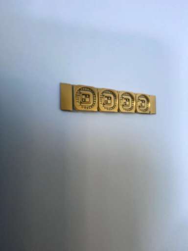
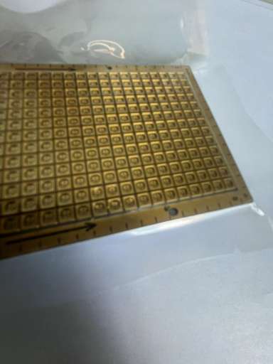
Multi-cavity PCB
Multi-cavity PCBs Manufacturer, Multiple Cavity PCBs are produced using high frequency and high speed mixed media materials or other materials. We control the depth of each Cavity according to the designer’s requirements, because this depth is important when assembling components.
Mixed dielectric Multi-cavity PCBs represent a sophisticated evolution in printed circuit board (PCB) technology, integrating multiple compartments with diverse functionalities onto a single board. Each cavity within the PCB serves as a dedicated space for distinct electronic components or circuits, enabling intricate system architectures within limited spatial constraints. This innovative design allows for the consolidation of various functionalities, such as analog, digital, power management, and communication circuits, into a compact and efficient platform. Mixed dielectric Multi-cavity PCBs find applications across diverse industries, including telecommunications, automotive, aerospace, medical devices, consumer electronics, and IoT (Internet of Things). They offer benefits such as enhanced functionality integration, reduced system complexity, improved thermal management, and optimized signal integrity. With their versatility and performance, Mixed dielectric Multi-cavity PCBs empower designers to realize advanced electronic systems with greater efficiency and reliability, catering to the evolving demands of modern technology.
What is a Multi-cavity PCB?
A multi-cavity PCB (Printed Circuit Board) refers to a type of circuit board design where there are multiple independent circuit cavities or compartments integrated into a single board. Each cavity can house different electronic components or circuits, allowing for compact and efficient designs, especially in applications where space is limited.
The main advantage of multi-cavity PCBs is their ability to integrate multiple functionalities into a single board, reducing overall system complexity, size, and cost. This approach can be particularly useful in electronics manufacturing, where space optimization and component integration are critical considerations.
Multi-cavity PCBs are commonly used in various electronic devices such as smartphones, tablets, wearable devices, IoT (Internet of Things) devices, and other compact electronic systems. They enable designers to pack more functionality into smaller form factors while maintaining efficient thermal management and signal integrity.
What are the Multi-cavity PCB Design Guidelines?
Designing multi-cavity PCBs requires careful consideration to ensure proper functionality, manufacturability, and reliability. Here are some guidelines to follow:
- Partitioning: Clearly define the boundaries of each cavity and allocate space for components, traces, and vias within each cavity. Consider the spatial requirements of components and their interconnections.
- Signal Integrity: Pay attention to signal integrity by minimizing signal crosstalk between cavities. Keep high-speed signal traces away from sensitive components and parallel traces to reduce interference.
- Power Distribution: Plan for efficient power distribution within each cavity to ensure stable voltage levels and minimize voltage drops. Use appropriate power planes and distribute power traces evenly to avoid hot spots.
- Thermal Management: Incorporate thermal management techniques such as thermal vias, heatsinks, and thermal pads to dissipate heat effectively, especially in densely populated cavities.
- Manufacturability: Optimize the layout for manufacturability by considering PCB fabrication and assembly processes. Ensure that cavity dimensions, component placements, and trace routing are compatible with manufacturing capabilities.
- EMI/EMC Considerations: Implement measures to mitigate electromagnetic interference (EMI) and ensure electromagnetic compatibility (EMC). This includes proper grounding, shielding, and layout techniques to minimize emissions and susceptibility.
- Accessibility: Design the PCB with accessibility in mind, ensuring that components within each cavity can be easily accessed for testing, troubleshooting, and maintenance.
- Mechanical Stability: Reinforce the PCB to maintain mechanical stability, especially if the design involves multiple stacked cavities or if the PCB will be subjected to mechanical stress.
- Documentation: Provide clear and comprehensive documentation, including cavity dimensions, component placement guidelines, layer stackup details, and routing constraints, to aid in PCB fabrication and assembly.
- Prototyping and Testing: Prototype and thoroughly test the multi-cavity PCB design to validate functionality, performance, and reliability before mass production.
By adhering to these guidelines, designers can create multi-cavity PCBs that meet the requirements for functionality, manufacturability, and reliability.
Multi-Cavity PCB
What is the Multi-cavity PCB Fabrication Process?
The fabrication process for multi-cavity PCBs shares similarities with that of standard PCBs but involves additional steps to accommodate multiple cavities. Here’s an overview of the multi-cavity PCB fabrication process:
- Design Preparation: Develop a detailed PCB design layout using CAD (Computer-Aided Design) software. Define the boundaries of each cavity, allocate space for components and traces, and establish routing paths.
- Material Selection: Choose the appropriate substrate material based on factors such as dielectric constant, thermal conductivity, and mechanical properties. Multi-cavity PCBs may require materials capable of supporting complex structures and multiple layers.
- Layer Stackup Design: Determine the layer stackup configuration considering the number of cavities, signal requirements, and manufacturing constraints. Arrange the layers to accommodate signal, power, and ground planes effectively.
- Circuit Imaging: Use photolithography or direct imaging techniques to transfer the PCB layout onto copper-clad laminate sheets. Create individual layer patterns for each cavity, including traces, pads, and vias.
- Lamination: Bond the individual layers together using heat and pressure to form a solid composite structure. This process creates the multilayer PCB stackup, with each layer containing circuitry for different cavities.
- Drilling: Drill holes for vias and component mounting pads at precise locations according to the PCB design. Ensure alignment accuracy to maintain connectivity between layers and cavities.
- Plating and Copper Deposition: Coat the drilled holes with conductive material through processes such as electroplating or chemical deposition. This step establishes electrical connections between different layers and facilitates signal transmission.
- Circuit Patterning: Apply a resist layer and use chemical etching to remove unwanted copper, leaving behind the desired circuit patterns for each cavity. Repeat this process for all layers, ensuring proper alignment and registration.
- Surface Finish: Apply a surface finish to protect exposed copper surfaces from oxidation and ensure solderability. Common surface finish options include HASL (Hot Air Solder Leveling), ENIG (Electroless Nickel Immersion Gold), and OSP (Organic Solderability Preservatives).
- Solder Mask Application: Apply solder mask ink over the entire PCB surface, leaving openings for component pads, vias, and electrical contacts. The solder mask protects the copper traces and enhances electrical insulation.
- Silkscreen Printing: Print component labels, reference designators, and other identifying markings onto the PCB surface using silkscreen printing. This step aids in component placement, assembly, and troubleshooting.
- Quality Assurance: Conduct thorough inspections and testing to verify the integrity, functionality, and reliability of the multi-cavity PCB. Inspect for defects, such as shorts, opens, or misalignments, and perform electrical testing to ensure proper connectivity.
- Final Finishing: Trim excess material, depanelize individual PCBs from the larger panel, and perform final cleaning and inspection. Prepare the multi-cavity PCBs for assembly and integration into electronic devices.
By following these steps, manufacturers can fabricate multi-cavity PCBs with precision and quality, meeting the requirements of complex electronic systems and applications.
Multi-Cavity PCB
How do you manufacture a Multi-cavity PCB?
Manufacturing a multi-cavity PCB involves several steps, from designing the layout to final assembly. Here’s a general overview of the manufacturing process:
- Design and Layout: Develop the PCB layout using computer-aided design (CAD) software. Define the boundaries of each cavity and allocate space for components, traces, and vias within each cavity.
- Material Selection: Choose the appropriate substrate material based on the application requirements. Multi-cavity PCBs often use materials like FR-4 (Flame Retardant 4), which offer good electrical properties and are cost-effective.
- Layer Stackup Design: Determine the layer stackup configuration considering the number of cavities and signal requirements. Arrange the layers to accommodate signal, power, and ground planes effectively.
- Circuit Imaging: Use photolithography or direct imaging techniques to transfer the PCB layout onto copper-clad laminate sheets. Create individual layer patterns for each cavity, including traces, pads, and vias.
- Drilling: Drill holes for vias and component mounting pads at precise locations according to the PCB design. Ensure alignment accuracy to maintain connectivity between layers and cavities.
- Plating and Copper Deposition: Coat the drilled holes with conductive material through processes such as electroplating or chemical deposition. This step establishes electrical connections between different layers and facilitates signal transmission.
- Circuit Patterning: Apply a resist layer and use chemical etching to remove unwanted copper, leaving behind the desired circuit patterns for each cavity. Repeat this process for all layers, ensuring proper alignment and registration.
- Surface Finish: Apply a surface finish to protect exposed copper surfaces from oxidation and ensure solderability. Common surface finish options include HASL (Hot Air Solder Leveling), ENIG (Electroless Nickel Immersion Gold), and OSP (Organic Solderability Preservatives).
- Solder Mask Application: Apply solder mask ink over the entire PCB surface, leaving openings for component pads, vias, and electrical contacts. The solder mask protects the copper traces and enhances electrical insulation.
- Silkscreen Printing: Print component labels, reference designators, and other identifying markings onto the PCB surface using silkscreen printing. This step aids in component placement, assembly, and troubleshooting.
- Component Placement and Soldering: Mount electronic components onto the PCB surface using pick-and-place machines. Ensure accurate placement and orientation of components, then solder them onto the PCB using reflow soldering or wave soldering techniques.
- Inspection and Testing: Conduct visual inspections and electrical testing to verify the integrity, functionality, and reliability of the multi-cavity PCB. Inspect for defects, such as shorts, opens, or misalignments, and perform functional testing to ensure proper operation.
- Final Finishing: Trim excess material, depanelize individual PCBs from the larger panel, and perform final cleaning and inspection. Prepare the multi-cavity PCBs for integration into electronic devices or systems.
By following these steps, manufacturers can produce high-quality multi-cavity PCBs that meet the requirements of various electronic applications.
How much should a Multi-cavity PCB cost?
The cost of a multi-cavity PCB can vary widely depending on several factors, including but not limited to:
- Complexity: The complexity of the PCB design, including the number of layers, the density of components, the size of the board, and the intricacy of the routing, significantly influences the cost.
- Material: The choice of substrate material and its specifications (e.g., thickness, dielectric constant) can impact the cost. High-performance materials may incur higher costs compared to standard FR-4.
- Manufacturing Process: The manufacturing processes involved, such as drilling, plating, etching, and surface finishing, contribute to the overall cost. Advanced processes or additional steps for impedance control or blind/buried vias may increase costs.
- Volume: The quantity of PCBs ordered typically affects the unit cost. Larger production runs may offer economies of scale, resulting in lower per-unit costs.
- Turnaround Time: Shorter lead times or expedited production may come at an additional cost due to prioritization and resource allocation.
- Supplier and Location: The choice of PCB manufacturer and their location can influence costs due to differences in labor costs, overhead expenses, and shipping fees.
- Additional Services: Optional services such as PCB assembly, testing, conformal coating, and component sourcing can increase the overall cost.
It’s essential to obtain quotes from multiple PCB manufacturers and evaluate them based on your specific requirements and budget constraints. Additionally, consider factors such as quality, reliability, lead time, and customer support when selecting a PCB supplier.
What is a Multi-cavity PCB base material?
The choice of base material for a multi-cavity PCB depends on various factors such as electrical performance, mechanical properties, thermal management requirements, and cost considerations. Common base materials used for multi-cavity PCBs include:
- FR-4 (Flame Retardant 4): FR-4 is the most widely used substrate material for PCBs due to its excellent electrical insulation properties, affordability, and availability. It offers good mechanical strength and is suitable for most general-purpose applications.
- High-Speed Materials: For applications requiring high-frequency signal transmission or impedance control, specialized materials such as high-frequency laminates (e.g., Rogers RO4000 series) may be used. These materials offer low dielectric loss, consistent electrical performance, and reduced signal distortion.
- High-Temperature Materials: In environments with elevated operating temperatures, thermally resistant substrates such as polyimide (e.g., Kapton) or high-temperature FR-4 variants may be employed. These materials can withstand higher temperatures without compromising electrical performance or mechanical integrity.
- Metal Core Materials: Multi-cavity PCBs designed for applications requiring efficient thermal dissipation often utilize metal core materials such as aluminum or copper-clad laminates. These materials offer superior thermal conductivity, allowing for effective heat dissipation from components and circuitry.
- Flexible Materials: For applications requiring flexibility or the ability to conform to non-planar surfaces, flexible substrates such as polyimide (e.g., Kapton) or polyester (e.g., PET) may be used. Flexible materials enable the creation of bendable or foldable PCBs suitable for compact and space-constrained designs.
The choice of base material should align with the specific requirements and performance criteria of the multi-cavity PCB, considering factors such as signal integrity, thermal management, mechanical stability, and cost-effectiveness. It’s essential to consult with PCB manufacturers and design engineers to select the most suitable base material for your application.
Which company makes Multi-cavity PCB?
The manufacturing of Multi-cavity PCBs is typically undertaken by specialized Printed Circuit Board (PCB) manufacturing companies. These companies usually possess advanced production equipment, extensive experience, and professional teams to meet diverse customer needs. Many well-known PCB manufacturers around the world offer production services for Multi-cavity PCBs, including Foxconn, TSMC, and Lixun Precision.
Our company is also a professional PCB manufacturer capable of producing various types of PCBs, including Mixed Multi-cavity PCBs. Mixed Multi-cavity PCBs refer to designs where multiple cavities or regions with different functions are integrated into the same PCB. This design allows for the integration of multiple different functional circuits on a single PCB, making electronic products more compact and efficient. Equipped with advanced production equipment and a skilled technical team, our company can customize various complex PCB designs according to customer requirements while ensuring product quality and reliability. We are committed to providing high-quality products and excellent services, meeting customers’ individual needs, and delivering reliable circuit solutions for their electronic products.
What are the 7 qualities of good customer service?
Good customer service is characterized by several key qualities that contribute to positive interactions and customer satisfaction. Here are seven qualities of good customer service:
- Responsiveness: Good customer service involves promptly addressing customer inquiries, concerns, and requests. Responding in a timely manner demonstrates attentiveness to customer needs and fosters trust and satisfaction.
- Empathy: Empathy is the ability to understand and share the feelings of customers. Good customer service representatives listen actively, demonstrate compassion, and acknowledge the customer’s emotions to provide personalized support and solutions.
- Professionalism: Professionalism encompasses courteous behavior, respectfulness, and adherence to company policies and standards. Customer service representatives should maintain a professional demeanor and communicate clearly and effectively with customers.
- Knowledgeability: Good customer service requires a thorough understanding of products, services, and policies. Customer service representatives should be knowledgeable about the company’s offerings and be able to provide accurate information and guidance to customers.
- Problem-solving skills: Effective problem-solving skills are essential for resolving customer issues and addressing complaints satisfactorily. Good customer service representatives identify root causes, offer creative solutions, and follow through to ensure customer needs are met.
- Patience: Patience is crucial when dealing with challenging or frustrated customers. Good customer service representatives remain calm, composed, and patient, even in difficult situations, to de-escalate conflicts and find mutually beneficial resolutions.
- Consistency: Consistency in service delivery builds customer trust and loyalty. Good customer service ensures that all customers receive the same level of quality assistance and support, regardless of the channel or representative they interact with.
By embodying these qualities, businesses can cultivate positive customer experiences, build strong relationships, and differentiate themselves in the competitive marketplace.
FAQs
What is a Mixed Multi-cavity PCB?
A Mixed Multi-cavity PCB is a type of printed circuit board (PCB) that integrates multiple cavities or compartments with different functionalities into a single board. Each cavity may house different electronic components or circuits, allowing for complex and versatile designs.
What are the advantages of Mixed Multi-cavity PCBs?
Mixed Multi-cavity PCBs offer several advantages, including compact design, efficient space utilization, reduced system complexity, and enhanced functionality integration. They also facilitate better thermal management and signal integrity.
What applications are suitable for Mixed Multi-cavity PCBs?
Mixed Multi-cavity PCBs are suitable for various applications across industries such as telecommunications, automotive, aerospace, medical devices, consumer electronics, and IoT (Internet of Things). They are ideal for products requiring compact designs with multiple integrated functionalities.
How are Mixed Multi-cavity PCBs designed?
The design process for Mixed Multi-cavity PCBs involves partitioning the board into multiple cavities, allocating space for components and traces within each cavity, and ensuring proper connectivity between cavities. Designers use CAD (Computer-Aided Design) software to create detailed layouts and optimize the placement of components.
What materials are used for Mixed Multi-cavity PCBs?
Mixed Multi-cavity PCBs can be manufactured using various substrate materials, including standard FR-4 (Flame Retardant 4), high-frequency laminates, high-temperature materials, and metal-core substrates. The choice of material depends on the specific requirements of the application.
How are Mixed Multi-cavity PCBs manufactured?
The manufacturing process for Mixed Multi-cavity PCBs involves similar steps to standard PCB fabrication, including material selection, layer stackup design, circuit imaging, drilling, plating, etching, solder mask application, component placement, soldering, inspection, and testing.
What considerations should be taken into account when designing Mixed Multi-cavity PCBs?
Designers should consider factors such as signal integrity, thermal management, mechanical stability, manufacturability, and cost-effectiveness when designing Mixed Multi-cavity PCBs. Collaboration with experienced PCB manufacturers is essential to ensure successful design implementation.