
Cavity PCB Manufacturing, Open Cavity, or buried cavity in the High speed and high frequency or other mixed pressure dielectric materials PCBs, Put the IC in the cavity area. We have made many types Cavity PCBs with high quality. and fast shiping time. Cavity PCBs, also known as Cavity Printed Circuit Boards, revolutionize electronic assembly by integrating components directly into the substrate. Featuring recessed areas within the PCB, these boards offer a compact and streamlined solution for various industries. By embedding components such as chips, sensors, or connectors directly into the PCB, Cavity PCBs reduce overall device size while enhancing reliability and performance. This innovative technology enables better thermal management, improved signal integrity, and enhanced protection for embedded components. Cavity PCBs find applications in diverse fields including telecommunications, aerospace, medical devices, automotive electronics, and consumer electronics. Designing and manufacturing Cavity PCBs require expertise in precision machining, advanced fabrication techniques, and careful consideration of thermal and electrical properties. With their ability to optimize space utilization and enhance electronic functionality, Cavity PCBs represent a significant advancement in PCB technology, driving innovation and efficiency in electronic product design and manufacturing.
What is Cavity PCB Technology?
Cavity PCB (Printed Circuit Board) technology refers to the process of creating a recessed area or cavity within a PCB substrate. This technique is used to embed components or modules directly into the PCB itself, rather than mounting them on the surface.
Here are some key aspects of Cavity PCB technology:
- Embedded Components: The main feature of cavity PCBs is the ability to embed components such as chips, sensors, or other electronic devices directly into the PCB substrate. This can reduce the overall size of the electronic device and improve its reliability by protecting the components from external elements.
- Reduced Size: By embedding components within the PCB, the overall size of the electronic device can be reduced. This is particularly advantageous in applications where space is limited, such as in portable electronics or wearable devices.
- Improved Performance: Embedding components within the PCB can also lead to improved electrical performance by reducing parasitic effects such as stray capacitance and inductance. This can result in higher speed operation and better signal integrity.
- Thermal Management: Cavity PCB technology can also be used for thermal management purposes. By embedding heat-generating components within the PCB substrate, heat dissipation can be improved, leading to better overall thermal performance and reliability.
- Complexity and Cost: Implementing cavity PCB technology can add complexity to the PCB manufacturing process, which may result in higher production costs. However, the benefits in terms of size reduction, performance improvement, and reliability can often justify the added cost.
Overall, cavity PCB technology offers a way to integrate components directly into the PCB substrate, providing benefits in terms of size reduction, performance improvement, and reliability in various electronic applications.
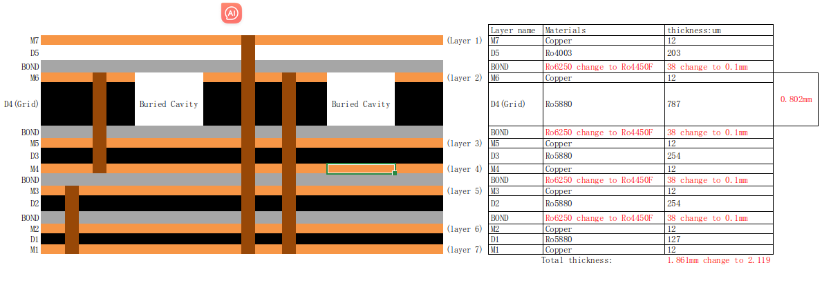
Buried cavity PCB
What are the Cavity PCB Design Guidelines?
Designing cavity PCBs requires careful consideration of various factors to ensure proper functionality, manufacturability, and reliability. Here are some key guidelines for cavity PCB design:
- Component Selection: Choose components suitable for embedding within the PCB substrate. These components should be flat and preferably have a low profile to fit well within the cavity without protruding excessively.
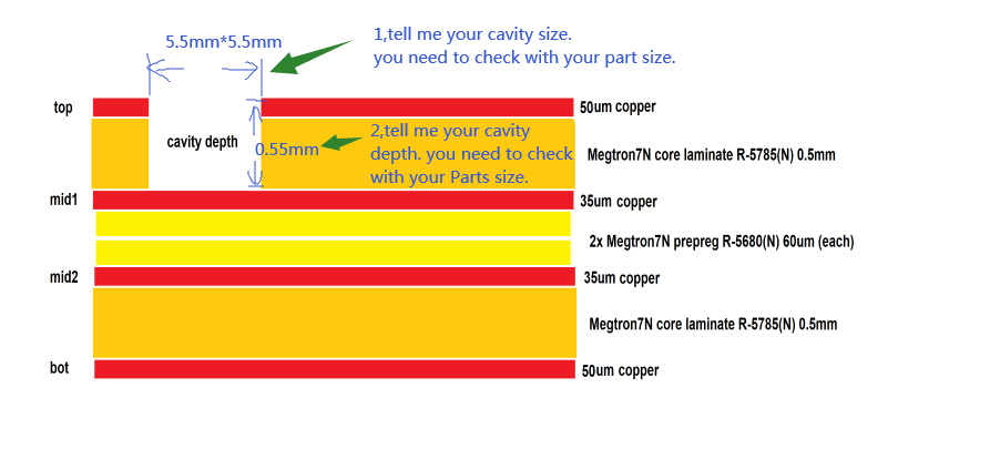
- Cavity Size and Shape: Determine the size and shape of the cavity based on the dimensions of the embedded components and any required clearance or spacing. Ensure that the cavity dimensions are accurately specified in the PCB design files.
- Cavity Depth: Consider the depth of the cavity to accommodate the height of the embedded components and any necessary clearance for soldering or assembly processes. The depth should provide sufficient space for the components while maintaining structural integrity.
- Cavity Wall Thickness: Ensure adequate wall thickness around the cavity to provide mechanical support and prevent flexing or damage during handling or assembly. The wall thickness should be sufficient to maintain structural integrity while minimizing material usage.
- Cavity Placement: Position the cavity within the PCB substrate to optimize layout and routing of traces while avoiding interference with other components or signal paths. Consider factors such as signal integrity, thermal management, and accessibility for testing and maintenance.
- Signal Routing: Plan the routing of traces around the cavity to minimize signal distortion and interference. Maintain appropriate clearance between traces and the cavity walls to prevent electrical shorting or coupling effects.
- Grounding and Shielding: Implement proper grounding and shielding techniques to minimize electromagnetic interference (EMI) and ensure signal integrity. Connect the cavity walls to ground planes or shielding layers as necessary to provide electromagnetic containment.
- Thermal Considerations: Evaluate thermal management requirements for components within the cavity and design the PCB layout accordingly. Provide adequate thermal vias, heat sinks, or thermal pads to dissipate heat effectively and maintain optimal operating temperatures.
- Manufacturability: Consider manufacturability aspects such as material selection, fabrication processes, and assembly techniques. Consult with PCB manufacturers early in the design process to ensure compatibility with cavity PCB requirements.
- Documentation: Clearly document cavity dimensions, tolerances, material specifications, and other relevant details in the PCB design files. Provide comprehensive assembly instructions and notes to guide manufacturing and assembly processes.
By following these guidelines, designers can create cavity PCBs that meet performance requirements, manufacturing constraints, and reliability standards for various electronic applications. Collaboration with experienced PCB manufacturers and adherence to best practices throughout the design process are essential for successful implementation of cavity PCB technology.
Open Cavity PCBs
What is the Cavity PCB Fabrication Process?
The fabrication process for cavity PCBs involves several steps, including substrate preparation, cavity creation, component placement, and assembly. Here’s a general overview of the cavity PCB fabrication process:
- Substrate Selection: Choose a suitable substrate material for the PCB based on factors such as mechanical strength, thermal conductivity, and dielectric properties. Common substrate materials include FR-4 (fiberglass-reinforced epoxy), ceramic, and flexible materials like polyimide.
- Circuit Design: Develop the PCB layout design using CAD (Computer-Aided Design) software, considering the placement of components, signal routing, and the location of the cavity. Ensure that the design meets the electrical and mechanical requirements of the application.
- Cavity Creation: Use specialized manufacturing techniques to create the cavity within the PCB substrate. This process typically involves CNC (Computer Numerical Control) milling or routing to remove material from the substrate, leaving behind the desired cavity shape and dimensions.
- Surface Preparation: Clean the substrate surface to remove any contaminants and prepare it for subsequent processes such as copper deposition and solder mask application. Surface cleaning may involve chemical cleaning, plasma treatment, or mechanical scrubbing.
- Copper Deposition: Apply a thin layer of copper onto the substrate surface using processes such as electroless copper deposition or sputtering. This copper layer serves as the conductive material for forming the PCB traces and pads.
- Circuit Patterning: Use photolithography or direct imaging techniques to transfer the PCB circuit pattern onto the copper layer. This involves applying a photoresist material to the substrate, exposing it to UV light through a photomask, and developing the resist to define the circuit traces and pads.
- Copper Etching: Remove unwanted copper from the substrate surface by etching using chemical solutions such as ferric chloride or ammonium persulfate. The etching process selectively removes copper, leaving behind the desired circuit pattern.
- Surface Finish: Apply a surface finish to the exposed copper traces and pads to protect them from oxidation and facilitate soldering during component assembly. Common surface finishes include HASL (Hot Air Solder Leveling), ENIG (Electroless Nickel Immersion Gold), and OSP (Organic Solderability Preservatives).
- Component Placement: Mount electronic components onto the PCB surface and within the cavity using automated pick-and-place machines or manual assembly techniques. Ensure proper alignment and orientation of components according to the PCB design.
- Soldering: Secure the components to the PCB surface by soldering them in place. This can be done using techniques such as reflow soldering, wave soldering, or hand soldering, depending on the specific requirements of the components and assembly process.
- Testing and Inspection: Conduct electrical testing and visual inspection to verify the functionality and quality of the assembled PCB. Test for continuity, shorts, and other defects using automated testing equipment, and visually inspect for any soldering or assembly issues.
- Final Finishing: Apply any final surface coatings or protective layers to the PCB to enhance durability and reliability. This may include applying conformal coatings, encapsulation materials, or labeling for identification purposes.
By following these steps, manufacturers can fabricate cavity PCBs that meet the required specifications for various electronic applications, ensuring functionality, reliability, and performance. Collaboration between PCB designers, fabricators, and assemblers is essential to optimize the fabrication process and achieve successful outcomes.
How do you manufacture a Cavity PCB?
Manufacturing a cavity PCB involves additional steps compared to traditional PCB fabrication due to the creation of the recessed area within the substrate. Here’s a detailed overview of the manufacturing process for cavity PCBs:
- Substrate Preparation:
– Select a suitable substrate material such as FR-4, ceramic, or flexible materials based on the application requirements.
– Cut the substrate material to the desired size and shape using precision cutting equipment.
- Cavity Creation:
– Use CNC (Computer Numerical Control) milling or routing machines to create the cavity within the substrate. The cavity’s size, shape, and depth should align with the design specifications.
– Ensure precise control over milling or routing parameters to achieve accurate cavity dimensions and a smooth cavity surface.
- Copper Deposition:
– Apply a thin layer of copper onto the substrate surface, including the cavity walls and floor. This can be done through processes such as electroless copper deposition or sputtering.
– The copper layer serves as the conductive material for forming the PCB traces and pads.
- Circuit Patterning:
– Apply a layer of photoresist material onto the copper-coated substrate.
– Expose the photoresist to UV light through a photomask, transferring the PCB circuit pattern onto the substrate.
– Develop the photoresist to remove the unexposed areas, leaving behind the desired circuit traces and pads on the substrate and within the cavity.
- Copper Etching:
– Remove unwanted copper from the substrate surface using chemical etching processes. The etching solution selectively dissolves the exposed copper, leaving behind the circuit traces and pads.
– Ensure precise control over etching parameters to maintain the integrity of the circuit pattern and minimize undercutting.
- Surface Finish:
– Apply a surface finish to the exposed copper traces and pads to protect them from oxidation and facilitate soldering during component assembly.
– Common surface finishes include HASL (Hot Air Solder Leveling), ENIG (Electroless Nickel Immersion Gold), and OSP (Organic Solderability Preservatives).
- Component Placement:
– Mount electronic components onto the PCB surface and within the cavity using automated pick-and-place machines or manual assembly techniques.
– Ensure proper alignment and orientation of components according to the PCB design.
- Soldering:
– Secure the components to the PCB surface by soldering them in place. This can be done using techniques such as reflow soldering, wave soldering, or hand soldering.
– Ensure adequate solder coverage and fillet formation for reliable electrical connections.
- Testing and Inspection:
– Conduct electrical testing and visual inspection to verify the functionality and quality of the assembled PCB.
– Test for continuity, shorts, and other defects using automated testing equipment.
– Visually inspect for any soldering or assembly issues, including component alignment and solder joint quality.
- Final Finishing:
– Apply any final surface coatings or protective layers to the PCB to enhance durability and reliability.
– This may include applying conformal coatings, encapsulation materials, or labeling for identification purposes.
By following these steps, manufacturers can produce cavity PCBs that meet the required specifications for various electronic applications, ensuring functionality, reliability, and performance. Collaboration between PCB designers, fabricators, and assemblers is essential to optimize the manufacturing process and achieve successful outcomes.
How much should a Cavity PCB cost?
The cost of a cavity PCB can vary significantly depending on various factors such as design complexity, materials used, fabrication techniques, component requirements, and manufacturing volume. Here are some key factors that influence the cost of cavity PCBs:
- Design Complexity: PCBs with complex designs, multiple layers, tight tolerances, and intricate cavity structures may require more time and specialized equipment to manufacture, resulting in higher costs.
- Materials: The choice of substrate material, copper thickness, surface finish, and any additional features such as impedance control or special dielectric properties can impact the cost of the PCB.
- Cavity Size and Depth: Larger or deeper cavities may require more material removal and additional processing steps, contributing to higher manufacturing costs.
- Manufacturing Techniques: The fabrication techniques used, such as CNC milling, laser drilling, or specialized surface treatments, can affect the overall cost of production.
- Component Assembly: The complexity of component placement, soldering processes, and testing requirements can influence the cost of PCB assembly.
- Volume: The manufacturing volume, or quantity of PCBs produced, often affects the unit cost. Higher volumes typically result in lower per-unit costs due to economies of scale.
- Lead Time: Expedited production or shorter lead times may incur additional costs for rush orders or premium services.
- Supplier Selection: Different PCB manufacturers may offer varying pricing structures, capabilities, and levels of service, so choosing the right supplier can impact overall costs.
It’s important to work closely with PCB manufacturers to obtain detailed quotes based on your specific design requirements and production volumes. Providing thorough documentation and discussing cost-saving strategies, such as optimizing design for manufacturability or adjusting material specifications, can help mitigate costs while ensuring the desired performance and quality of the cavity PCBs.
What is Cavity PCB base material?
The base material used for cavity PCBs is typically chosen based on the specific requirements of the application, including electrical performance, mechanical strength, thermal properties, and cost considerations. Common materials used for cavity PCB substrates include:
- FR-4 (Flame Retardant-4): FR-4 is a widely used substrate material for PCBs due to its excellent electrical insulation properties, mechanical strength, and relatively low cost. It consists of a woven fiberglass cloth impregnated with an epoxy resin binder.
- Rogers RO4000 Series: Rogers Corporation offers a range of high-performance laminates specifically designed for RF/microwave applications. These materials offer low dielectric constant (Dk) and low loss tangent (Df), making them suitable for high-frequency circuitry often found in cavity PCBs.
- Ceramic Substrates: Ceramic materials such as alumina (Al2O3) or aluminum nitride (AlN) are used in applications requiring high thermal conductivity and excellent electrical properties. Ceramic substrates are commonly used in power electronics and high-power RF applications.
- Flexible Materials: For applications requiring flexibility or conformability, flexible substrates such as polyimide (e.g., Kapton) or polyester (e.g., PET) may be used. These materials are suitable for applications where space constraints or mechanical flexibility are critical.
- Metal Core PCBs (MCPCB): Metal core PCBs feature a metal substrate, typically aluminum or copper, which provides excellent thermal conductivity. MCPCBs are often used in applications requiring efficient heat dissipation, such as LED lighting and power electronics.
- High-Frequency Laminates: For RF/microwave applications operating at high frequencies, specialized laminates with low-loss dielectric materials and controlled impedance properties may be used. These materials offer excellent signal integrity and performance at higher frequencies.
When selecting the base material for a cavity PCB, factors such as dielectric properties, thermal conductivity, mechanical strength, dimensional stability, and compatibility with fabrication processes must be carefully considered to ensure the desired performance and reliability of the final product.
Which company manufactures Cavity PCBs?
Cavity PCBs are typically manufactured by professional Printed Circuit Board (PCB) manufacturing companies. Some well-known PCB manufacturers and Electronic Manufacturing Services (EMS) providers have advanced technology and equipment to produce high-quality Cavity PCBs. These companies usually have extensive experience and expertise to meet the needs of various industries and applications.
As a professional PCB manufacturer, our company has advanced equipment and an experienced team to produce high-quality Cavity PCBs. Our manufacturing process is carefully designed to ensure that each step meets strict quality standards and customer requirements. Our engineering team has extensive experience and expertise to provide customized solutions to meet specific customer needs.
Our manufacturing capabilities cover various types of Cavity PCBs, including multi-layer PCBs, high-frequency PCBs, rigid-flex PCBs, and more. We can produce Cavity PCBs in different sizes, shapes, and materials according to customer design requirements and specifications. Our production process strictly follows the ISO quality management system to ensure that each product meets customer requirements and industry standards.
In addition to high-quality products, our company also focuses on customer service and communication. Our team is committed to building long-term partnerships with customers, understanding their needs, and providing timely support and solutions. We can provide customized quotes and technical support according to customer requirements to ensure customer satisfaction and trust.
In summary, our company has the technology, equipment, and experience required to produce high-quality Cavity PCBs, as well as a professional team and excellent customer service. We are willing to cooperate with customers, grow together, and provide the best solutions and support to customers.
What are the 7 qualities of good customer service?
Good customer service is characterized by several key qualities that contribute to positive customer experiences and satisfaction. Here are seven qualities of good customer service:
- Responsiveness: Good customer service involves being prompt and responsive to customer inquiries, requests, and concerns. Responding to customer queries in a timely manner demonstrates attentiveness and a commitment to addressing their needs promptly.
- Empathy: Empathy is essential in understanding and acknowledging customers’ emotions, concerns, and perspectives. Customer service representatives who show empathy demonstrate genuine care and concern for customers’ experiences, which helps build trust and rapport.
- Professionalism: Professionalism encompasses maintaining a courteous, respectful, and polite demeanor in all customer interactions. Customer service representatives should conduct themselves professionally, regardless of the nature or complexity of the customer’s issue.
- Knowledgeability: Good customer service requires having a thorough understanding of the products or services offered, as well as company policies, procedures, and solutions to common issues. Knowledgeable representatives can provide accurate information and effective assistance to customers.
- Problem-Solving Skills: Effective problem-solving skills are crucial for resolving customer issues and addressing their concerns satisfactorily. Customer service representatives should be proactive in identifying solutions, taking ownership of problems, and following through until resolution is achieved.
- Adaptability: Good customer service involves being flexible and adaptable to meet the diverse needs and preferences of customers. Representatives should be able to adjust their approach, communication style, and problem-solving strategies based on individual customer situations.
- Consistency: Consistency is key to delivering excellent customer service consistently across all interactions and touchpoints. Customers should receive the same level of quality service regardless of who they interact with or how they choose to engage with the company.
By embodying these qualities, organizations can foster positive relationships with customers, enhance satisfaction and loyalty, and differentiate themselves in a competitive marketplace.
FAQs (Frequently Asked Questions)
What is a Cavity PCB?
A Cavity PCB, or Cavity Printed Circuit Board, is a type of PCB that features a recessed area or cavity within the substrate. This cavity allows for the embedding of components directly into the PCB, resulting in a more compact and integrated electronic assembly.
What are the benefits of Cavity PCBs?
Cavity PCBs offer several benefits, including reduced overall size of electronic devices, improved reliability by protecting components, enhanced thermal management, and improved electrical performance by minimizing parasitic effects.
Which industries commonly use Cavity PCBs?
Cavity PCBs find applications across various industries, including telecommunications, aerospace, medical devices, automotive electronics, consumer electronics, and more. Any application requiring compact and reliable electronic assemblies can benefit from Cavity PCB technology.
What types of components can be embedded in Cavity PCBs?
Cavity PCBs can accommodate a wide range of components, including integrated circuits (ICs), sensors, connectors, passive components (resistors, capacitors), and more. Components are typically selected based on the specific requirements of the application.
What materials are used in Cavity PCBs?
The choice of materials for Cavity PCBs depends on the application requirements. Common substrate materials include FR-4, ceramic, flexible materials (polyimide), and metal core PCBs. The selection of materials influences factors such as electrical performance, thermal management, and mechanical strength.
What are the design considerations for Cavity PCBs?
Designing Cavity PCBs requires careful consideration of factors such as cavity size and shape, component placement, thermal management, signal routing, and manufacturability. Collaboration between PCB designers and manufacturers is essential to optimize the design for performance and reliability.